TL DD10802
COP680CCOP681CCOP682CCOP880CCOP881CCOP882CCOP980CCOP981CCOP982C
Microcontrollers
August 1996
COP680C COP681C COP682C COP880C COP881C
COP882C COP980C COP981C COP982C
Microcontrollers
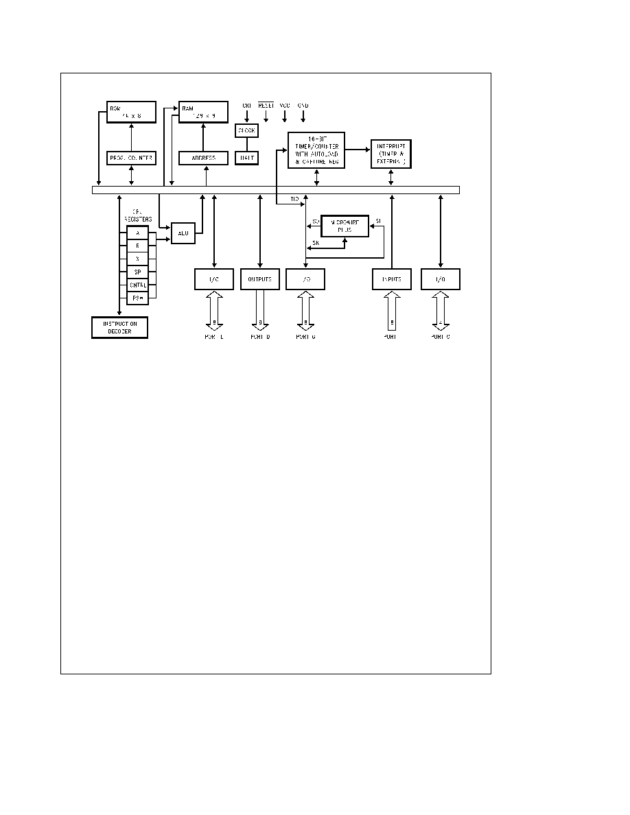
General Description
The COP680C COP681C COP682C COP880C COP881C
COP882C COP980C COP981C and COP982C are mem-
bers of the COPS
TM
microcontroller family They are fully
static parts
fabricated using double-metal silicon gate
microCMOS technology This low cost microcontroller is a
complete microcomputer containing all system timing inter-
rupt logic ROM RAM and I O necessary to implement
dedicated control functions in a variety of applications Fea-
tures include an 8-bit memory mapped architecture MI-
CROWIRE PLUS
TM
serial I O a 16-bit timer counter with
capture register and a multi-sourced interrupt Each I O pin
has software selectable options to adapt the device to the
specific application The part operates over a voltage range
of 2 5 to 6 0V High throughput is achieved with an efficient
regular instruction set operating at a 1 microsecond per in-
struction rate
Key Features
Y
16-bit multi-function timer supporting
PWM mode
External event counter mode
Input capture mode
Y
4 kbytes of ROM
Y
128 bytes of RAM
I O Features
Y
Memory mapped I O
Y
Software selectable I O options (TRI-STATE
Push-
Pull Weak Pull-Up Input High Impedance Input)
Y
High current outputs (8 pins)
Y
Schmitt trigger inputs on Port G
Y
MICROWIRE PLUS serial I O
Y
Packages
20 DIP SO with 16 I O pins
28 DIP SO with 24 I O pins
40 DIP 36 I O pins
44 PLCC 36 I O pins
CPU Instruction Set Features
Y
1 ms instruction cycle time
Y
Three multi-source interrupts servicing
External interrupt with selectable edge
Timer interrupt
Software interrupt
Y
Versatile and easy to use instruction set
Y
8-bit Stack Pointer (SP)
stack in RAM
Y
Two 8-bit Register Indirect Data Memory Pointers
(B and X)
Fully Static CMOS
Y
Low current drain (typically
k
1 mA)
Y
Single supply operation 2 5V to 6 0V
Y
Temperature ranges 0 C to 70 C
b
40 C to
a
85 C
b
55 C to
a
125 C
Development Support
Y
Emulation and OTP devices
Y
Real time emulation and full program debug offered by
MetaLink's development system
TRI-STATE
is a registered trademark of National Semiconductor Corporation
COPS
TM
HPC
TM
MICROWIRE
TM
and MICROWIRE PLUS
TM
are trademarks of National Semiconductor Corporation
iceMASTER
TM
is a trademark of MetaLink Corporation
PC-XT
and PC-AT
are registered trademarks of International Business Machines Corporation
C1996 National Semiconductor Corporation
RRD-B30M106 Printed in U S A
http
www national com
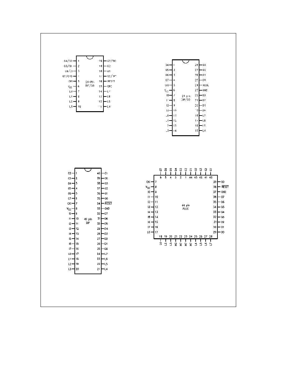
Connection Diagrams
Dual-In-Line Package
TL DD 10802 � 23
Top View
Order Number COP882C-XXX N COP982C-XXX N
COP882C-XXX WM COP982C-XXX WM
COP982C-XXX N or COP982CH-XXX WM
Dual-In-Line Package (N)
and 28 Wide SO (WM)
TL DD 10802 � 5
Top View
Order Number COP881C-XXX N COP981C-XXX N
COP881C-XXX WM COP981C-XXX WM
COP981CH-XXX N or COP981CH-XXX WM
Dual-In-Line Package
TL DD 10802 � 4
Top View
Order Number COP680C-XXX N COP880C-XXX N
COP980C-XXX N or COP980CH-XXX N
Plastic Chip Carrier
TL DD 10802 � 3
Top View
Order Number COP680C-XXX V COP880C-XXX V
COP980C-XXX V or COP980CH-XXX V
FIGURE 3 Connection Diagrams
http
www national com
3
COP980C COP981C COP982C
Absolute Maximum Ratings
If Military Aerospace specified devices are required
please contact the National Semiconductor Sales
Office Distributors for availability and specifications
Supply Voltage (V
CC
)
7V
Voltage at any Pin
b
0 3V to V
CC
a
0 3V
Total Current into V
CC
Pin (Source)
50 mA
Total Current out of GND Pin (Sink)
60 mA
Storage Temperature Range
b
65 C to
a
140 C
Note Absolute maximum ratings indicate limits beyond
which damage to the device may occur DC and AC electri-
cal specifications are not ensured when operating the de-
vice at absolute maximum ratings
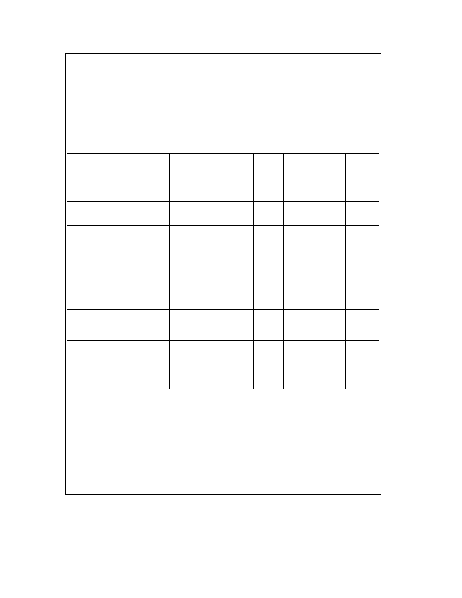
DC Electrical Characteristics
COP98xC 0 C
s
T
A
s
a
70 C unless otherwise specified
Parameter
Condition
Min
Typ
Max
Units
Operating Voltage
98XC
2 3
4 0
V
98XCH
4 0
6 0
V
Power Supply Ripple (Note 1)
Peak to Peak
0 1 V
CC
V
Supply Current
CKI
e
10 MHz
V
CC
e
6V tc
e
1 ms
6 0
mA
CKI
e
4 MHz
V
CC
e
6V tc
e
2 5 ms
4 4
mA
CKI
e
4 MHz
V
CC
e
4 0V tc
e
2 5 ms
2 2
mA
CKI
e
1 MHz
V
CC
e
4 0V tc
e
10 ms
1 4
mA
(Note 2)
HALT Current
V
CC
e
6V CKI
e
0 MHz
k
0 7
8
m
A
(Note 3)
V
CC
e
4 0V CKI
e
0 MHz
k
0 4
5
m
A
Input Levels
RESET CKI
Logic High
0 9 V
CC
V
Logic Low
0 1 V
CC
V
All Other Inputs
Logic High
0 7 V
CC
V
Logic Low
0 2 V
CC
V
Hi-Z Input Leakage
V
CC
e
6 0V
b
1 0
a
1 0
m
A
Input Pullup Current
V
CC
e
6 0V V
IN
e
0V
b
40
b
250
m
A
G Port Input Hysteresis
0 35 V
CC
V
Output Current Levels
D Outputs
Source
V
CC
e
4 5V V
OH
e
3 8V
b
0 4
mA
V
CC
e
2 3V V
OH
e
1 6V
b
0 2
mA
Sink
V
CC
e
4 5V V
OL
e
1 0V
10
mA
V
CC
e
2 3V V
OL
e
0 4V
2
mA
All Others
Source (Weak Pull-Up)
V
CC
e
4 5V V
OH
e
3 2V
b
10
b
110
m
A
V
CC
e
2 3V V
OH
e
1 6V
b
2 5
b
33
m
A
Source (Push-Pull Mode)
V
CC
e
4 5V V
OH
e
3 8V
b
0 4
mA
V
CC
e
2 3V V
OH
e
1 6V
b
0 2
Sink (Push-Pull Mode)
V
CC
e
4 5V V
OL
e
0 4V
1 6
mA
V
CC
e
2 3V V
OL
e
0 4V
0 7
TRI-STATE Leakage
V
CC
e
6 0V
b
1 0
a
1 0
m
A
Allowable Sink Source
Current Per Pin
D Outputs (Sink)
15
mA
All Others
3
mA
Maximum Input Current (Note 4)
Without Latchup (Room Temp)
Room Temp
g
100
mA
RAM Retention Voltage Vr
500 ns Rise and
(Note 5)
Fall Time (Min)
2 0
V
Input Capacitance
7
pF
Load Capacitance on D2
1000
pF
http
www national com
4
COP980C COP981C COP982C
DC Electrical Characteristics
(Continued)
Note 1
Rate of voltage change must be less than 0 5V ms
Note 2
Supply current is measured after running 2000 cycles with a square wave CKI input CKO open inputs at rails and outputs open
Note 3
The HALT mode will stop CKI from oscillating in the RC and the Crystal configurations Test conditions All inputs tied to V
CC
L C and G ports TRI-STATE
and tied to ground all outputs low and tied to ground
Note 4
Pins G6 and RESET are designed with a high voltage input network for factory testing These pins allow input voltages greater than V
CC
and the pins will
have sink current to V
CC
when biased at voltages greater than V
CC
(the pins do not have source current when biased at a voltage below V
CC
) The effective
resistance to V
CC
is 750X (typ) These two pins will not latch up The voltage at the pins must be limited to less than 14V
Note 5
To maintain RAM integrity the voltage must not be dropped or raised instantaneously
AC Electrical Characteristics
0 C
s
T
A
s
a
70 C unless otherwise specified
Parameter
Condition
Min
Typ
Max
Units
Instruction Cycle Time (tc)
Crystal Resonator or External
V
CC
t
4 0V
1
DC
m
s
(Div-by 10)
2 3V
s
V
CC
s
4 0V
2 5
DC
m
s
R C Oscillator Mode
V
CC
t
4 0V
3
DC
m
s
(Div-by 10)
2 3V
s
V
CC
s
4 0V
7 5
DC
m
s
CKI Clock Duty Cycle (Note 6)
fr
e
Max
40
60
%
Rise Time (Note 6)
fr
e
10 MHz Ext Clock
12
ns
Fall Time (Note 6)
fr
e
10 MHz Ext Clock
8
ns
Inputs
t
SETUP
V
CC
t
4 0V
200
ns
2 3V
s
V
CC
s
4 0V
500
ns
t
HOLD
V
CC
t
4 0V
60
ns
2 3V
s
V
CC
s
4 0V
150
ns
Output Propagation Delay
C
L
e
100 pF R
L
e
2 2 kX
t
PD1
t
PD0
SO SK
V
CC
t
4 0V
0 7
m
s
2 3V
s
V
CC
s
4 0V
1 75
m
s
All Others
V
CC
t
4 0V
1
m
s
2 3V
s
V
CC
s
4 0V
2 5
m
s
MICROWIRE
TM
Setup Time (t
UWS)
20
ns
MICROWIRE Hold Time (t
UWH)
56
ns
MICROWIRE Output
Propagation Delay (t
UPD
)
220
ns
Input Pulse Width
Interrupt Input High Time
t
C
Interrupt Input Low Time
t
C
Timer Input High Time
t
C
Timer Input Low Time
t
C
Reset Pulse Width
1 0
m
s
Note 6
Parameter characterized but not production tested
http
www national com
5