COP888CL
8-Bit Microcontroller
General Description
The following part numbers are pin count and tempera-
ture
variations
of
the
COP888CL:
COP688CL,
COP684CL, COP884CL, COP988CL, COP984CL.
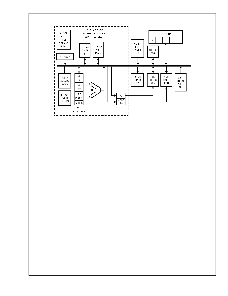
The COP888 family of microcontrollers uses an 8-bit single
chip core architecture fabricated with National Semiconduc-
tor's M
2
CMOS
TM
process technology. The COP888CL is a
member of this expandable 8-bit core processor family of
microcontrollers.
It is a fully static part, fabricated using double-metal silicon
gate microCMOS technology. Features include an 8-bit
memory mapped architecture, MICROWIRE/PLUS serial
I/O, two 16-bit timer/counters supporting three modes (Pro-
cessor Independent PWM generation, External Event
counter, and Input Capture mode capabilities), and two
power savings modes (HALT and IDLE), both with a multi-
sourced wakeup/interrupt capability. This multi-sourced in-
terrupt capability may also be used independent of the HALT
or IDLE modes. Each I/O pin has software selectable con-
figurations. The device operates over a voltage range of
2.5V to 6V. High throughput is achieved with an efficient,
regular instruction set operating at a maximum of 1 µs per
instruction rate.
Key Features
n
Two 16-bit timers, each with two 16-bit registers
supporting:
-- Processor Independent PWM mode
-- External Event counter mode
-- Input Capture mode
n
4 kbytes of on-chip ROM
n
128 bytes of on-chip RAM
Additional Peripheral Features
n
Idle Timer
n
Multi-input Wake Up (MIWU) with optional interrupts (8)
n
WATCHDOG and Clock Monitor logic
n
MICROWIRE/PLUS
TM
serial I/O
I/O Features
n
Memory mapped I/O
n
Software selectable I/O options ( TRI-STATE Output,
Push-Pull Output, Weak Pull-Up Input, High Impedance
Input)
n
High current outputs
n
Schmitt trigger inputs on port G
n
Packages:
-- 44 PLCC with 40 I/O pins
-- 40 DIP with 36 I/O pins
-- 28 DIP with 24 I/O pins
-- 28 SO with 24 I/O pins
CPU/Instruction Set Feature
n
1 µs instruction cycle time
n
Ten multi-source vectored interrupts servicing
-- External Interrupt with selectable edge
-- Idle Timer T0
-- Timers (Each with 2 interrupts)
-- MICROWIRE/PLUS
-- Multi-Input Wake Up
-- Software Trap
-- Default VIS (default interrupt)
n
Versatile and easy to use instruction set
n
8-bit Stack Pointer (SP) -- stack in RAM
n
Two 8-bit Register Indirect Data Memory Pointers (B, X)
Fully Static CMOS
n
Low current drain (typically
<
1 µA)
n
Single supply operation: 2.5V to 6.0V
n
Temperature ranges: 0∞C to +70∞C, -40∞C to +85∞C,
-55∞C to +125∞C
Development Support
n
Emulation and OTP devices
n
Real time emulation and full program debug offered by
MetaLink Development System
MICROWIRE/PLUS
TM
, M2CMOS
TM
, COPS
TM
microcontrollers, and MICROWIRE
TM
are trademarks of National Semiconductor Corporation.
iceMASTER
TM
is a trademark of MetaLink Corporation.
September 2000
COP888CL
8-Bit
Microcontroller
© 2001 National Semiconductor Corporation
DS009766
www.national.com
Connection Diagrams
Plastic Chip Carrier
DS009766-2
Top View
Order Number COP688CL-XXX/V, COP888CL-XXX/V,
COP988CL-XXX/V or COP988CLH-XXX/V
See NS Plastic Chip Package Number V44A
Dual-In-Line Package
DS009766-4
Top View
Order Number COP688CL-XXX/N, COP888CL-XXX/N,
COP988CL-XXX/N or COP988CLH-XXX/N
See NS Molded Package Number N40A
Dual-In-Line Package
DS009766-5
Top View
Order Number COP688CL-XXX/N, COP884CL-XXX/N, COP984CL-XXX/N or COP984CLH-XXX/N
See NS Molded Package Number N28B
Order Number COP684CL-XXX/WM,
COP884CL-XXX/WM, COP984CL-XXX/WM,
or COP984CLHXXX/WM
See NS Surface Mount Package Number M28B
FIGURE 2. Connection Diagrams
COP888CL
www.national.com
3
Absolute Maximum Ratings
(Note 2)
If Military/Aerospace specified devices are required,
please contact the National Semiconductor Sales Office/
Distributors for availability and specifications.
Supply Voltage (V
CC
)
7V
Voltage at Any Pin
-0.3V to V
CC
+ 0.3V
Total Current into V
CC
Pin (Source)
100 mA
Total Current out of GND Pin (Sink)
110 mA
Storage Temperature Range
-65∞C to +140∞C
Note 2:
Absolute maximum ratings indicate limits beyond which damage to
the device may occur. DC and AC electrical specifications are not ensured
when operating the device at absolute maximum ratings.
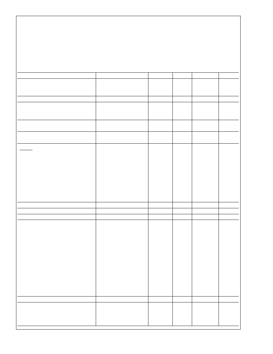
DC Electrical Characteristics
COP98XCL: 0∞C
T
A
+ 70∞C unless otherwise specified.
Parameter
Conditions
Min
Typ
Max
Units
Operating Voltage
COP98XCL
2.5
4.0
V
COP98XCLH
4.0
6.0
V
Power Supply Ripple (Note 3)
Peak-to-Peak
0.1 V
CC
V
Supply Current (Note 4)
CKI = 10 MHz
V
CC
= 6V, t
c
= 1 µs
12.5
mA
CKI = 4 MHz
V
CC
= 4V, t
c
= 2.5 µs
2.5
mA
HALT Current (Note 5)
V
CC
= 6V, CKI = 0 MHz
<
0.7
8
µA
V
CC
= 4V, CKI = 0 MHz
<
0.4
5
µA
IDLE Current
CKI = 10 MHz
V
CC
= 6V, t
c
= 1 µs
3.5
mA
Input Levels
RESET
Logic High
0.8 V
CC
V
Logic Low
0.2 V
CC
V
CKI (External and Crystal Osc. Modes)
Logic High
0.7 V
CC
V
Logic Low
0.2 V
CC
V
All Other Inputs
Logic High
0.7 V
CC
V
Logic Low
0.2 V
CC
V
Hi-Z Input Leakage
V
CC
= 6V
-1
+1
µA
Input Pullup Current
V
CC
= 6V, V
IN
= 0V
-40
-250
µA
G and L Port Input Hysteresis
0.35 V
CC
V
Output Current Levels
D Outputs
Source
V
CC
= 4V, V
OH
= 3.3V
-0.4
mA
V
CC
= 2.5V, V
OH
= 1.8V
-0.2
mA
Sink
V
CC
= 4V, V
OL
= 1V
10
mA
V
CC
= 2.5V, V
OL
= 0.4V
2.0
mA
All Others
Source (Weak Pull-Up Mode)
V
CC
= 4V, V
OH
= 2.7V
-10
-100
µA
V
CC
= 2.5V, V
OH
= 1.8V
-2.5
-33
µA
Source (Push-Pull Mode)
V
CC
= 4V, V
OH
= 3.3V
-0.4
mA
V
CC
= 2.5V, V
OH
= 1.8V
-0.2
mA
Sink (Push-Pull Mode)
V
CC
= 4V, V
OL
= 0.4V
1.6
mA
V
CC
= 2.5V, V
OL
= 0.4V
0.7
mA
TRI-STATE Leakage
V
CC
= 6.0V
-1
+1
µA
Allowable Sink/Source
Current per Pin
D Outputs (Sink)
15
mA
All others
3
mA
COP888CL
www.national.com
5