 | –≠–ª–µ–∫—Ç—Ä–æ–Ω–Ω—ã–π –∫–æ–º–ø–æ–Ω–µ–Ω—Ç: COP888EG | –°–∫–∞—á–∞—Ç—å:  PDF PDF  ZIP ZIP |
COP888xG/CS Family
8-Bit CMOS ROM Based Microcontrollers with 4k to 24k
Memory, Comparators and USART
General Description
Note: COP8SG devices are form-fit-function compatible su-
persets of the COP888xG/CL/CS Family devices, and are
replacements for these in new designs, and design up-
grades with minimum effort.
The COP888xG ROM based microcontrollers are highly inte-
grated COP8
TM
Feature core devices with larger memory (4k
to 24k) and advanced features including two Analog com-
parators. These single-chip CMOS devices are suited for
more complex applications requiring a full featured controller
with a range of memory sizes, low EMI (except EG), com-
parators, and a full-duplex USART. Pin and software com-
patible (different V
CC
range) 8k toor 32k OTP (One Time
Programmable) versions are available (COP8SGx7 Family).
Erasable windowed versions are available for use with a
range of software and hardware development tools.
Family features include an 8-bit memory mapped architec-
ture, 10 MHz CKI with 1µs instruction cycle, three multi-
function
16-bit
timer/counters,
full-duplex
USART,
MICROWIRE/PLUS
TM
serial I/O, two Analog comparators,
two power saving HALT/IDLE modes, idle timer, MIWU, high
current outputs, software selectable I/O options, WATCH-
DOG
TM
timer and Clock Monitor, low EMI 2.5V to 5.5V opera-
tion, and 28/40/44 pin packages.
Devices included in this datasheet are:
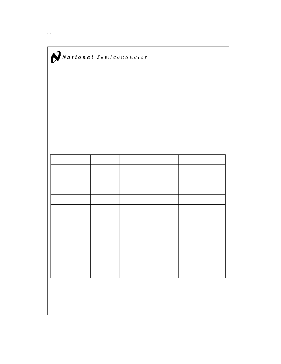
Device
Memory
(bytes)
RAM
(bytes)
I/O
Pins
Packages
Temperature
Comments
COP684CS
4k ROM
192
24
28 DIP/SOIC
-55 to +125∞C
4.5V - 5.5V
COP884CS
4k ROM
192
24
28 DIP/SOIC
-40 to +85∞C
COP984CS
4k ROM
192
24
28 DIP/SOIC
-0 to +70∞C
2.5V - 4.0V, CSH=4.0V - 6.0V
COP688CS
4k ROM
192
36/40
40 DIP, 44 PLCC
-55 to +125∞C
4.5V - 5.5V
COP888CS
4k ROM
192
36/40
40 DIP, 44 PLCC
-40 to +85∞C
COP988CS
4k ROM
192
36/40
40 DIP, 44 PLCC
-0 to +70∞C
2.5V - 4.0V, CSH=4.0V - 6.0V
COP884CG
4k ROM
128
24
28 DIP/SOIC
-40 to +85∞C
2.5V - 6.0V
COP888CG
4k ROM
128
34/38
40 DIP, 44 PLCC
-40 to +85∞C
2.5V - 6.0V
COP684EG
4k ROM
256
24
28 DIP, SOIC
-55 to +125∞C
4.5V - 5.5V
COP884EG
4k ROM
256
24
28 DIP, SOIC
-40 to +85∞C
COP984EG
4k ROM
256
24
28 DIP, SOIC
0 to +70∞C
2.5V - 4.0V, EGH=4.0 - 6.0V
COP688EG
8k ROM
256
36/40
40 DIP, 44 PLCC
-55 to +125∞C
4.5V - 5.5V
COP888EG
8k ROM
256
36/40
40 DIP, 44
PLCC/PQFP
-40 to +85∞C
COP988EG
8k ROM
256
36/40
40 DIP, 44 PLCC
0 to +70∞C
2.5V - 4.0V, EGH=4.0 - 6.0V
COP688GG
16k ROM
512
36/40
40 DIP, 44
PLCC/PQFP
-55 to +125∞C
4.5V - 5.5V
COP888GG
16k ROM
512
36/40
40 DIP, 44
PLCC/PQFP
-40 to +85∞C
COP688HG
20k ROM
512
36/40
40 DIP, 44 PLCC
-55 to +125∞C
4.5V - 5.5V
COP888HG
20k ROM
512
36/40
40 DIP, 44 PLCC
-40 to +85∞C
COP688KG
24k ROM
512
36/40
40 DIP, 44 PLCC
-55 to +125∞C
4.5V - 5.5V
COP888KG
24k ROM
512
36/40
40 DIP, 44 PLCC
-40 to +85∞C
Key Features
n
Full duplex USART
n
Three 16-bit timers, each with two 16-bit registers
supporting:
-- Processor Independent PWM mode
-- External Event counter mode
-- Input Capture mode
n
Quiet design (low radiated emissions)
n
4 to 24 kbytes on-board ROM
n
128 to 512 bytes on-board RAM
COP8
TM
, MICROWIRE/PLUS
TM
, and WATCHDOG
TM
are trademarks of National Semiconductor Corporation.
TRI-STATE
Æ
is a registered trademark of National Semiconductor Corporation.
iceMASTER
Æ
is a registered trademark of MetaLink Corporation.
July 1999
COP888xG/CS
Family,
8-Bit
CMOS
ROM
Based
Microcontrollers
with
4k
to
24k
Memory,
Comparators
and
USART
© 1999 National Semiconductor Corporation
DS012829
www.national.com
Key Features
(Continued)
Additional Peripheral Features
n
Idle Timer
n
Multi-Input Wake-Up (MIWU) with optional interrupts (8)
n
Two analog comparators (one for the CS series)
n
WATCHDOG and Clock Monitor logic
n
MICROWIRE/PLUS serial I/O
I/O Features
n
Memory mapped I/O
n
Software selectable I/O options (TRI-STATE
Æ
Output,
Push-Pull Output, Weak Pull-Up Input, High Impedance
Input)
n
Up to 8 high current outputs
n
Schmitt trigger inputs on ports G and L
n
Packages:
-- 44 PQFP with 40 I/O pins
-- 44 PLCC with 40 I/O pins
-- 40 DIP with 36 I/O pins
-- 28 DIP/SOIC with 24 I/O pins
CPU/Instruction Set Features
n
1 µs instruction cycle time
n
Versatile and easy to use instruction set
n
Up to fourteen multi-source vectored interrupts servicing
-- External Interrupt with selectable edge
-- Idle Timer T0
-- Three Timers (one timer for the CS series)(each with
2 interrupts)
-- MICROWIRE/PLUS
-- Multi-Input Wake-Up
-- Software Trap
-- USART (2)
-- Default VIS (default interrupt)
n
8-bit Stack Pointer SP -- (stack in RAM)
n
Two 8-bit Register Indirect Data Memory Pointers
(B and X)
Fully Static CMOS
n
Two power saving modes: HALT and IDLE
n
Low current drain (typically
<
1 µA)
n
Single supply operation: 2.5V≠5.5V (COP88x)
n
Temperature ranges:
0∞C to +70∞C, -40∞C to +85∞C, and -55∞C to +125∞C
Development Support
n
Emulation and OTP devices
n
Real time emulation and full program debug offered by
MetaLink's Development System
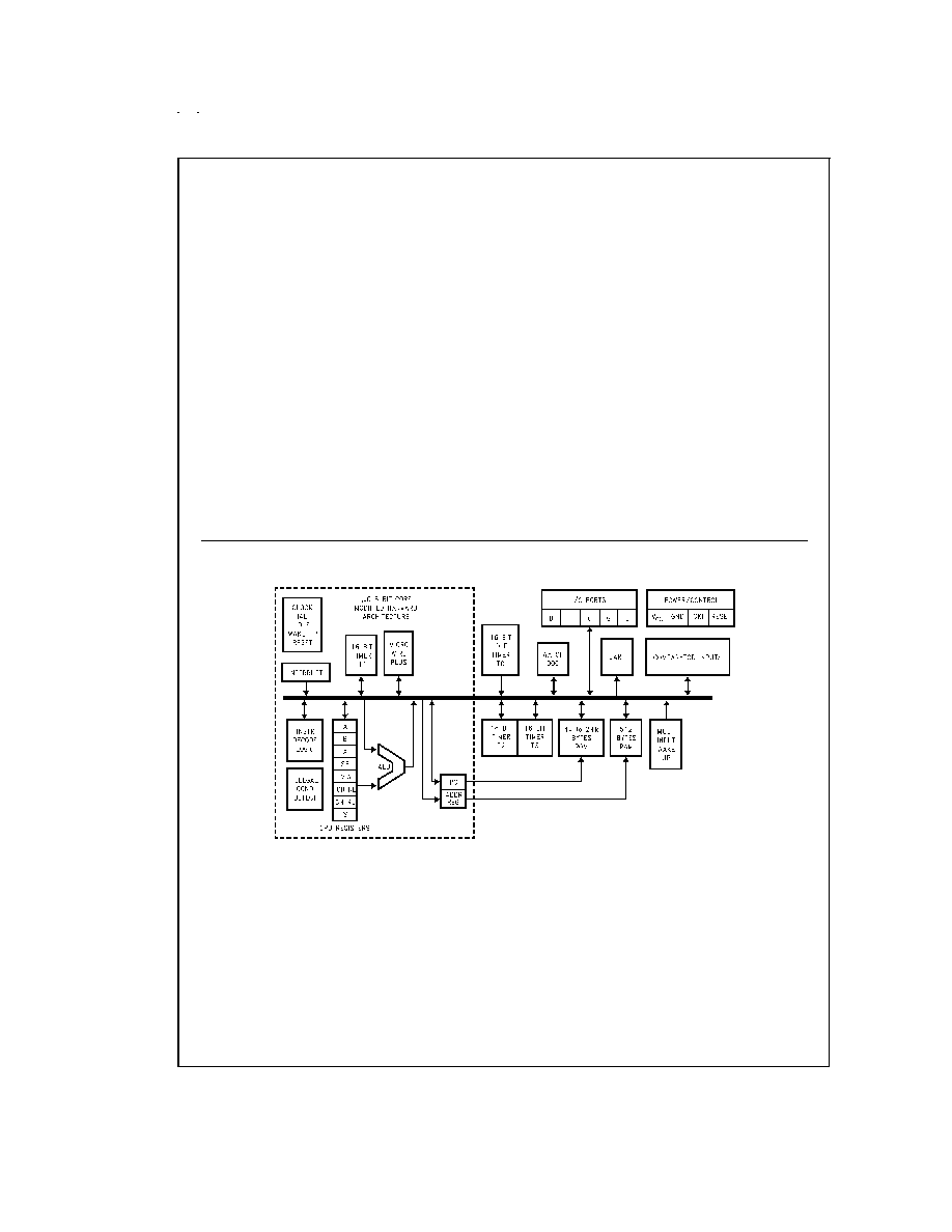
Block Diagram
DS012829-1
FIGURE 1. COP888xG Block Diagram
www.national.com
2
Connection Diagrams
DS012829-4
Top View
Order Number COP884CS-XXX/WM,
COP984CS-XXX/WM,
COP984CSH-XXX/WM, COP684CS-XXX/WM,
COP884CG-XXX/WM,
COP884EG-XXX/WM or
COP884CS-XXX/N, COP984CS-XXX/N,
COP984CSH-XXX/N, COP884CG-XXX/N,
COP884EG-XXX/N
See NS Package Number M28B or N28A
Dual-In-Line Package
DS012829-3
Top View
Order Number COP888CS-XXX/N, COP988CS-XXX/N,
COP688CS-XXX/N,
COP988CSH-XXX/N, COP888CG-XXX/N,
COP688EG-XXX/N, COP888GG-XXX/N,
COP688GG-XXX/N, COP888GG-XXX/N,
COP688HG-XXX/N, COP888HG-XXX/N,
COP688KG-XXX/N, or COP888KG-XXX/N
See NS Package Number N40A
Plastic Chip Carrier
DS012829-2
Top View
Order Number COP688CS-XXX/V, COP888CS-XXX/V,
COP988CS/CSH-XXX/V, COP688EG-XXX/V,
COP888EG-XXX/V, COP988EG-XXX/V,
COP888CG-XXX/V,
COP688GG-XXX/V, COP888GG-XXX/V,
COP688HG-XXX/V, COP888HG-XXX/V,
COP688KG-XXX/V, or COP888KG-XXX/V
See NS Package Number V44A
DS012829-43
Top View
Order Number COP888EG-XXX/VEJ,
COP688GG-XXX/VEJ, COP888GG-XXX/VEJ,
See NS Package Number VEJ44A
FIGURE 2. Connection Diagrams
www.national.com
3
Connection Diagrams
(Continued)
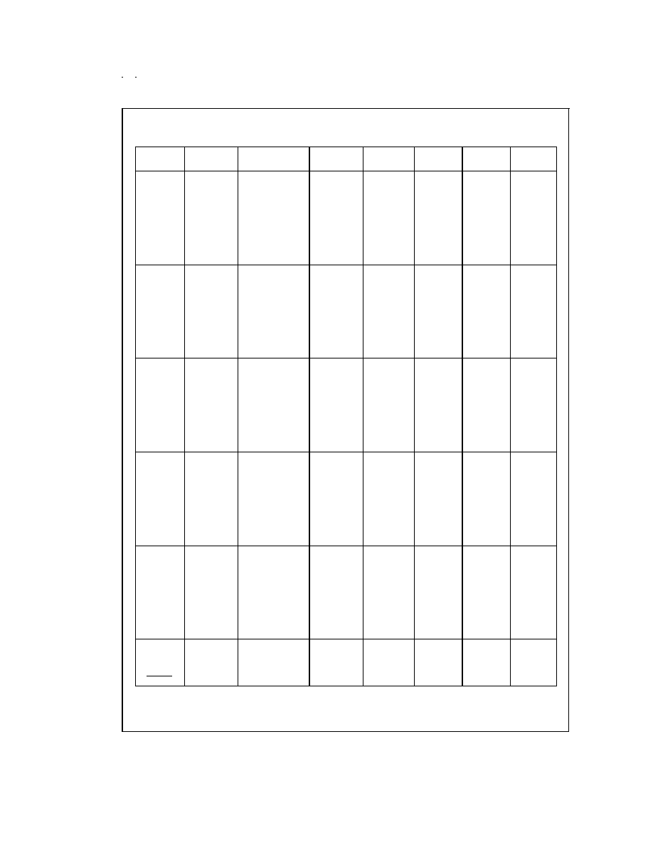
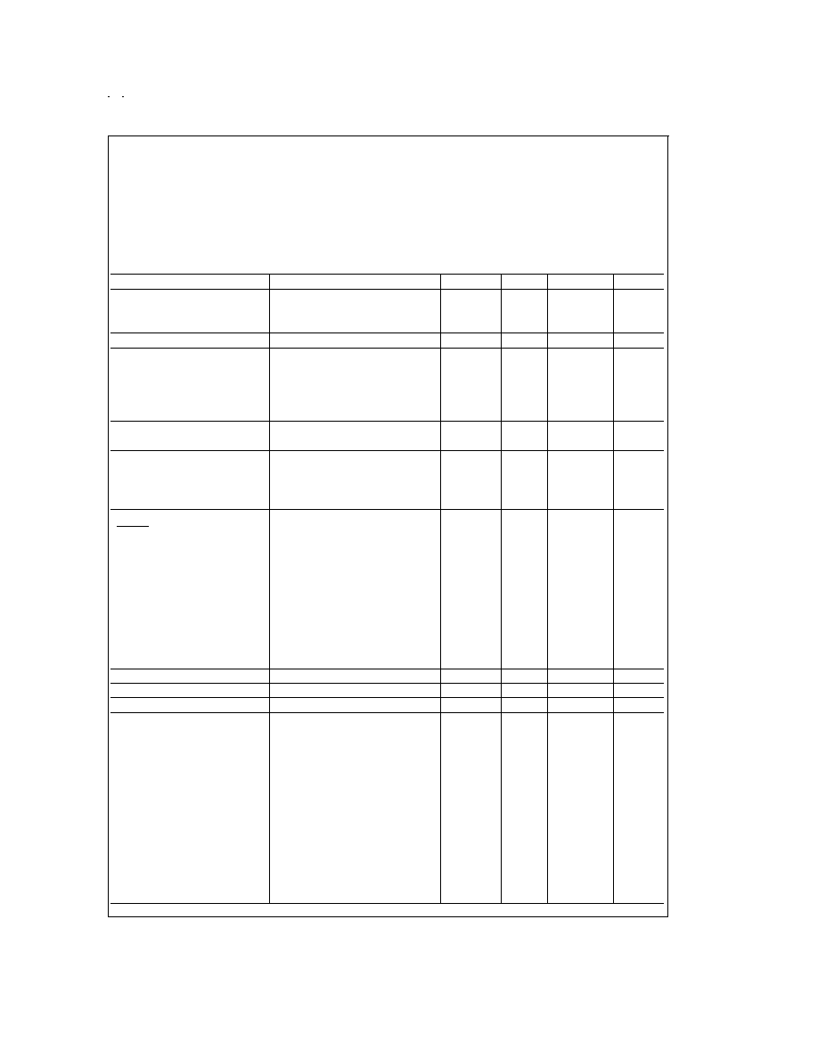
Pinouts for 28-, 40- and 44-Pin Packages
Port
Type
Alt. Fun
Alt. Fun
28-Pin
40-Pin
44-Pin
44-Pin
DIP/SO
DIP
PLCC
PQFP
L0
I/O
MIWU
11
17
17
11
L1
I/O
MIWU
CKX
12
18
18
12
L2
I/O
MIWU
TDX
13
19
19
13
L3
I/O
MIWU
RDX
14
20
20
14
L4
I/O
MIWU
T2A*
15
21
25
19
L5
I/O
MIWU
T2B*
16
22
26
20
L6
I/O
MIWU
T3A*
17
23
27
21
L7
I/O
MIWU
T3B*
18
24
28
22
G0
I/O
INT
25
35
39
33
G1
WDOUT
26
36
40
34
G2
I/O
T1B
27
37
41
35
G3
I/O
T1A
28
38
42
36
G4
I/O
SO
1
3
3
41
G5
I/O
SK
2
4
4
42
G6
I
SI
3
5
5
43
G7
I/CKO
HALT Restart
4
6
6
44
D0
O
19
25
29
23
D1
O
20
26
30
24
D2
O
21
27
31
25
D3
O
22
28
32
26
D4
O
29
33
7
D5
O
30
34
8
D6
O
31
35
9
D7
O
32
36
10
I0
I
7
9
9
27
I1
I
COMP1IN-
8
10
10
28
I2
I
COMP1IN+
9
11
11
29
I3
I
COMP1OUT
10
12
12
30
I4
I
COMP2IN-*
13
13
3
I5
I
COMP2IN+*
14
14
4
I6
I
COMP2OUT*
15
15
5
I7
I
16
16
6
C0
I/O
39
43
37
C1
I/O
40
44
38
C2
I/O
1
1
39
C3
I/O
2
2
40
C4
I/O
21
15
C5
I/O
22
16
C6
I/O
23
17
C7
I/O
24
18
V
CC
6
8
8
2
GND
23
33
37
31
CKI
5
7
7
1
RESET
24
34
38
32
Note 1:
*
Not available on the CS series
www.national.com
4
Absolute Maximum Ratings
(Note 4)
If Military/Aerospace specified devices are required,
please contact the National Semiconductor Sales Office/
Distributors for availability and specifications.
Supply Voltage (V
CC
)
7V
Voltage at Any Pin
-0.3V to V
CC
+ 0.3V
Total Current into V
CC
Pin (Source)
100 mA
Total Current out of GND Pin (Sink)
110 mA
Storage Temperature Range
-65∞C to +140∞C
Note 2:
Absolute maximum ratings indicate limits beyond which damage to
the device may occur. DC and AC electrical specifications are not ensured
when operating the device at absolute maximum ratings.
DC Electrical Characteristics 98xEG and 98xCS:
0∞C
T
A
+70∞C unless otherwise specified
Parameter
Conditions
Min
Typ
Max
Units
Operating Voltage
COP98xCS, COP98xEG
2.5
4.0
V
COP98xCSH, COP98xEGH
4.0
6.0
V
Power Supply Ripple (Note 6)
Peak-to-Peak
0.1 V
CC
V
Supply Current (Note 7)
CKI = 10 MHz
V
CC
= 6.0V, t
c
= 1 µs
12.5
mA
CKI = 4 MHz
V
CC
= 6.0V, t
c
= 2.5 µs
5.5
mA
CKI = 4 MHz
V
CC
= 4V, t
c
= 2.5 µs
2.5
mA
CKI = 1 MHz
V
CC
= 4V, t
c
= 10 µs
1.4
mA
HALT Current (Note 8)
V
CC
= 6.0V, CKI = 0 MHz
<
0.7
8
µA
V
CC
= 4V, CKI = 0 MHz
<
0.3
4
µA
IDLE Current
CKI = 10 MHz
V
CC
= 6.0V, t
c
= 1 µs
3.5
mA
CKI = 4 MHz
V
CC
= 6.0V, t
c
= 2.5 µs
2.5
mA
CKI = 1 MHz
V
CC
= 4V, t
c
= 10 µs
0.7
mA
Input Levels (V
IH
, V
IL
)
RESET
Logic High
0.8 V
CC
V
Logic Low
0.2 V
CC
V
CKI (External adn Crystal Osc.
Modes)
Logic High
0.7 V
CC
V
Logic Low
0.2 V
CC
V
All Other Inputs
Logic High
0.7 V
CC
V
Logic Low
0.2 V
CC
V
Hi-Z Input Leakage
V
CC
= 6.0V, V
IN
= 0V
-1
+1
µA
Input Pullup Current
V
CC
= 6.0V, V
IN
= 0V
-40
-250
µA
G and L Port Input Hysteresis
(Note 10)
0.35 V
CC
V
Output Current Levels
D Outputs
Source
V
CC
= 4V, V
OH
= 3.3V
-0.4
mA
V
CC
= 2.5V, V
OH
= 1.8V
-0.2
mA
Sink
V
CC
= 4V, V
OL
= 1V
10
mA
V
CC
= 2.5V, V
OL
= 0.4V
2.0
mA
All Others
Source (Weak Pull-Up Mode)
V
CC
= 4V, V
OH
= 2.7V
-10
-100
µA
V
CC
= 2.5V, V
OH
= 1.8V
-2.5
-33
µA
Source (Push-Pull Mode)
V
CC
= 4V, V
OH
= 3.3V
-0.4
mA
V
CC
= 2.5V, V
OH
= 1.8V
-0.2
mA
Sink (Push-Pull Mode)
V
CC
= 4V, V
OL
= 0.4V
1.6
mA
V
CC
= 2.5V, V
OL
= 0.4V
0.7
mA
www.national.com
5