COP8AME9
8-Bit CMOS Flash Microcontroller with 8k Memory, Dual
Op Amps, Virtual EEPROM, Temperature Sensor, 10-Bit
A/D and Brownout Reset
1.0 General Description
The COP8AME9 Flash microcontroller is a highly integrated
COP8
TM
Feature core device, with 8k Flash memory and
advanced features including Virtual EEPROM, dual Op
Amps (one programmable gain), temperature sensor, A/D,
High Speed Timers, USART, and Brownout Reset. The
COP8AME9 has True In-System Programmable Flash
memory with high-endurance (100k erase/write cycles), and
is well suited for applications requiring real-time data collec-
tion and processing, multiple sensory interface, and remote
monitoring. The same device is used for development, pre-
production and volume production with a range of COP8
software and hardware development tools.
Device described in this datasheet:
Device
Flash
Program
Memory
(bytes)
RAM
(bytes)
Brownout
Voltage
I/O
Pins
Packages
Temperature
COP8AME9
8k
512
4.17 to 4.5V
21
28 DIP/SOIC
-40�C to +85�C
2.0 Features
KEY FEATURES
n
8 kbytes Flash Program Memory with High Security
n
512 bytes SRAM
n
10-bit Successive Approximation Analog to Digital
Converter (up to 6 external channels)
n
Op Amp Specification:
-- One programmable gain (1, 2, 5, 10, 20, 49, 98) with
adjustable offset voltage nulling
-- One general purpose with all I/O terminals accessible
-- 1 MHz GBW
-- Low offset voltage
-- High input impedance
-- Rail-to-rail input/output
n
Temperature Sensing Diode
n
True In-System Programmability of Flash Memory with
100k erase/write cycles
n
Dual Clock Operation providing Enhanced Power Save
Modes � HALT/IDLE
n
100% Precise Analog Emulation
n
Single supply operation: 4.5V�5.5V
n
Three 16-bit timers:
-- Timers T2 and T3 can operate at 50 ns resolution
-- Processor Independent PWM mode
-- External Event counter mode
-- Input Capture mode
n
Brownout Reset
n
20 high sink-current I/Os
n
USART
n
Virtual EEPROM using Flash Program Memory
n
7 input analog MUX with selectable output destination
OTHER FEATURES
n
Quiet Design (low radiated emissions)
n
Multi-Input Wake-up with optional interrupts
n
MICROWIRE/PLUS (Serial Peripheral Interface
Compatible)
n
Clock Doubler for 20 MHz operation from 10 MHz
Oscillator
n
Thirteen multi-source vectored interrupts servicing:
-- External Interrupt
-- USART (2)
-- Idle Timer T0
-- Three Timers (each with 2 interrupts)
-- MICROWIRE/PLUS Serial peripheral interface
-- Multi-Input Wake-Up
-- Software Trap
n
Idle Timer with programmable interrupt interval
n
8-bit Stack Pointer SP (stack in RAM)
n
Two 8-bit Register Indirect Data Memory Pointers
n
True bit manipulation
n
WATCHDOG and Clock Monitor logic
n
Software selectable I/O options
-- TRI-STATE Output/High Impedance Input
-- Push-Pull Output
-- Weak Pull-Up Input
n
Schmitt trigger inputs on I/O ports
n
Temperature range: �40�C to +85�C
n
Packaging: 28 DIP, and 28 SOIC
COP8
TM
is a trademark of National Semiconductor Corporation.
PRELIMINARY
February 2004
COP8AME9
8-Bit
CMOS
Flash
Based
Microcontroller
with
8k
Memory
,
Dual
Op
Amps,
V
irtual
EEPROM,
T
emperature
Sensor
,
10-Bit
A/D
and
Brownout
Reset
� 2004 National Semiconductor Corporation
DS200063
www.national.com
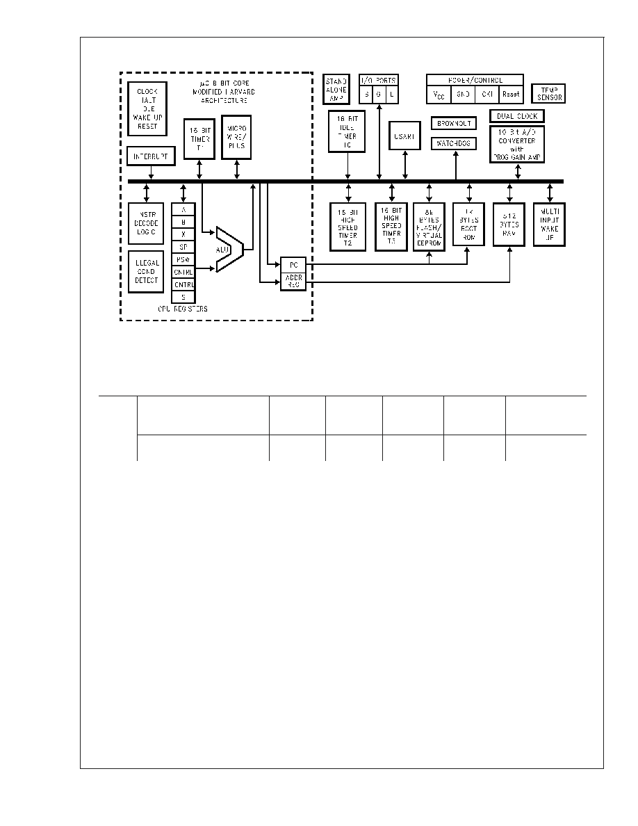
3.0 Block Diagram
20006301
4.0 Ordering Information
Part Numbering Scheme
COP8
AM
E
9
E
NA
8
Family and
Feature Set
Indicator
Program
Memory
Size
Program
Memory
Type
No. Of Pins
Package
Type
Temperature
AM = 4.17V - 4.5V Brownout
E = 8k
9 = Flash
E = 28 Pin
NA = DIP
MW = SOIC
8 = -40 to +85�C
COP8AME9
www.national.com
2

Table of Contents
1.0 General Description ..................................................................................................................................... 1
2.0 Features ....................................................................................................................................................... 1
3.0 Block Diagram .............................................................................................................................................. 2
4.0 Ordering Information .................................................................................................................................... 2
5.0 Connection Diagram .................................................................................................................................... 6
6.0 Architectural Overview ................................................................................................................................. 8
6.1 EMI REDUCTION ...................................................................................................................................... 8
6.2 IN-SYSTEM PROGRAMMING AND VIRTUAL EEPROM ........................................................................ 8
6.3 DUAL CLOCK AND CLOCK DOUBLER ................................................................................................... 8
6.4 TRUE IN-SYSTEM EMULATION .............................................................................................................. 8
6.5 ARCHITECTURE
..................................................................................................................................... 8
6.6 INSTRUCTION SET
................................................................................................................................. 8
6.6.1 Key Instruction Set Features ............................................................................................................... 8
6.6.2 Single Byte/Single Cycle Code Execution
......................................................................................... 8
6.6.3 Many Single-Byte, Multi-Function Instructions .................................................................................... 8
6.6.4 Bit-Level Control .................................................................................................................................. 9
6.6.5 Register Set ......................................................................................................................................... 9
6.7 PACKAGING/PIN EFFICIENCY ................................................................................................................ 9
7.0 Absolute Maximum Ratings ....................................................................................................................... 10
8.0 Electrical Characteristics ............................................................................................................................ 10
9.0 Pin Descriptions ......................................................................................................................................... 15
9.1 EMULATION CONNECTION ................................................................................................................... 16
10.0 Functional Description .............................................................................................................................. 16
10.1 CPU REGISTERS ................................................................................................................................. 16
10.2 PROGRAM MEMORY ........................................................................................................................... 17
10.3 DATA MEMORY .................................................................................................................................... 17
10.4 DATA MEMORY SEGMENT RAM EXTENSION .................................................................................. 17
10.4.1 Virtual EEPROM .............................................................................................................................. 18
10.5 OPTION REGISTER ............................................................................................................................. 18
10.6 SECURITY ............................................................................................................................................ 19
10.7 RESET ................................................................................................................................................... 19
10.7.1 External Reset ................................................................................................................................. 20
10.7.2 On-Chip Brownout Reset ................................................................................................................. 20
10.8 OSCILLATOR CIRCUITS ...................................................................................................................... 21
10.8.1 Oscillator .......................................................................................................................................... 21
10.8.2 Clock Doubler .................................................................................................................................. 22
10.9 CONTROL REGISTERS ....................................................................................................................... 22
10.9.1 CNTRL Register (Address X'00EE) ................................................................................................. 22
10.9.2 PSW Register (Address X'00EF) ..................................................................................................... 22
10.9.3 ICNTRL Register (Address X'00E8) ................................................................................................ 23
10.9.4 T2CNTRL Register (Address X'00C6) ............................................................................................. 23
10.9.5 T3CNTRL Register (Address X'00B6) ............................................................................................. 23
10.9.6 HSTCR Register (Address X'00AF) ................................................................................................ 23
10.9.7 ITMR Register (Address X'00CF) .................................................................................................... 23
10.9.8 ENAD Register (Address X'00CB) .................................................................................................. 23
11.0 In-System Programming ........................................................................................................................... 24
11.1 INTRODUCTION ................................................................................................................................... 24
11.2 FUNCTIONAL DESCRIPTION .............................................................................................................. 24
11.3 REGISTERS .......................................................................................................................................... 24
11.3.1 ISP Address Registers ..................................................................................................................... 24
11.3.2 ISP Read Data Register .................................................................................................................. 24
11.3.3 ISP Write Data Register ................................................................................................................... 24
11.3.4 ISP Write Timing Register ................................................................................................................ 25
11.4 MANEUVERING BACK AND FORTH BETWEEN FLASH MEMORY AND BOOT ROM ..................... 25
11.5 FORCED EXECUTION FROM BOOT ROM ......................................................................................... 26
11.6 RETURN TO FLASH MEMORY WITHOUT HARDWARE RESET ....................................................... 26
11.7 MICROWIRE/PLUS ISP ........................................................................................................................ 26
11.8 USER ISP AND VIRTUAL E
2
................................................................................................................ 27
11.9 RESTRICTIONS ON SOFTWARE WHEN CALLING ISP ROUTINES IN BOOT ROM ....................... 29
11.10 FLASH MEMORY DURABILITY CONSIDERATIONS ........................................................................ 29
12.0 Timers ....................................................................................................................................................... 30
12.1 TIMER T0 (IDLE TIMER) ...................................................................................................................... 30
COP8AME9
www.national.com
3

Table of Contents
(Continued)
12.1.1 ITMR Register .................................................................................................................................. 31
12.2 TIMER T1, TIMER T2, AND TIMER T3 ................................................................................................ 31
12.2.1 Timer Operating Speeds .................................................................................................................. 31
12.2.2 Mode 1. Processor Independent PWM Mode ................................................................................. 31
12.2.3 Mode 2. External Event Counter Mode ........................................................................................... 32
12.2.4 Mode 3. Input Capture Mode .......................................................................................................... 32
12.3 TIMER CONTROL FLAGS .................................................................................................................... 33
12.4 TIMER T2 OPERATION IN IDLE MODE .............................................................................................. 35
12.4.1 Timer T2 Clocking Scheme ............................................................................................................. 35
13.0 Power Saving Features ............................................................................................................................ 36
13.1 POWER SAVE MODE CONTROL REGISTER .................................................................................... 36
13.2 OSCILLATOR STABILIZATION ............................................................................................................. 37
13.3 HIGH SPEED MODE OPERATION ...................................................................................................... 37
13.3.1 High Speed Halt Mode .................................................................................................................... 37
13.3.1.1 Entering The High Speed Halt Mode ......................................................................................... 37
13.3.1.2 Exiting The High Speed Halt Mode ........................................................................................... 37
13.3.1.3 HALT Exit Using Reset .............................................................................................................. 37
13.3.1.4 HALT Exit Using Multi-Input Wake-up ....................................................................................... 37
13.3.1.5 Options ....................................................................................................................................... 38
13.3.2 High Speed Idle Mode ..................................................................................................................... 38
13.4 DUAL CLOCK MODE OPERATION ...................................................................................................... 39
13.4.1 Dual Clock HALT Mode ................................................................................................................... 39
13.4.1.1 Entering The Dual Clock Halt Mode .......................................................................................... 39
13.4.1.2 Exiting The Dual Clock Halt Mode ............................................................................................. 39
13.4.1.3 HALT Exit Using Reset .............................................................................................................. 39
13.4.1.4 HALT Exit Using Multi-Input Wake-up ....................................................................................... 39
13.4.1.5 Options ....................................................................................................................................... 39
13.4.2 Dual Clock Idle Mode ...................................................................................................................... 39
13.5 LOW SPEED MODE OPERATION ....................................................................................................... 40
13.5.1 Low Speed HALT Mode ................................................................................................................... 40
13.5.1.1 Entering The Low Speed Halt Mode ......................................................................................... 40
13.5.1.2 Exiting The Low Speed Halt Mode ............................................................................................ 40
13.5.1.3 HALT Exit Using Reset .............................................................................................................. 40
13.5.1.4 HALT Exit Using Multi-Input Wake-up ....................................................................................... 40
13.5.1.5 Options ....................................................................................................................................... 40
13.5.2 Low Speed Idle Mode ...................................................................................................................... 41
13.6 MULTI-INPUT WAKE-UP ...................................................................................................................... 42
14.0 USART ..................................................................................................................................................... 42
14.1 USART CONTROL AND STATUS REGISTERS ................................................................................... 43
14.2 DESCRIPTION OF USART REGISTER BITS ...................................................................................... 43
14.3 ASSOCIATED I/O PINS ........................................................................................................................ 44
14.4 USART OPERATION ............................................................................................................................ 45
14.4.1 Asynchronous Mode ........................................................................................................................ 45
14.4.2 Synchronous Mode .......................................................................................................................... 45
14.5 FRAMING FORMATS ............................................................................................................................ 45
14.6 USART INTERRUPTS .......................................................................................................................... 46
14.7 BAUD CLOCK GENERATION .............................................................................................................. 46
14.8 EFFECT OF HALT/IDLE ....................................................................................................................... 48
14.9 DIAGNOSTIC ........................................................................................................................................ 48
14.10 ATTENTION MODE ............................................................................................................................. 48
14.11 BREAK GENERATION ........................................................................................................................ 48
15.0 A/D Converter ........................................................................................................................................... 49
15.1 9.1 OPERATING MODES ..................................................................................................................... 49
15.1.1 A/D Control Register ........................................................................................................................ 49
15.1.1.1 Channel Select ........................................................................................................................... 49
15.1.1.2 Multiplexor Output Select ........................................................................................................... 50
15.1.1.3 Mode Select ............................................................................................................................... 51
15.1.1.4 Prescaler Select ......................................................................................................................... 51
15.1.1.5 Busy Bit ...................................................................................................................................... 51
15.1.2 A/D Result Registers ....................................................................................................................... 51
15.2 PROGRAMMABLE GAIN AMPLIFIER .................................................................................................. 52
COP8AME9
www.national.com
4

Table of Contents
(Continued)
15.2.1 Programmable Gain Amplifier Settling Time ................................................................................... 52
15.2.2 Programmable Gain Amplifier Offset Calibration ............................................................................. 53
15.2.3 Trimming the Offset on the Programmable Gain Amplifier ............................................................. 53
15.3 A/D OPERATION ................................................................................................................................... 54
15.3.1 Prescaler .......................................................................................................................................... 54
15.4 ANALOG INPUT AND SOURCE RESISTANCE CONSIDERATIONS .................................................. 54
16.0 Temperature Sensor ................................................................................................................................. 55
16.1 GENERAL DESCRIPTION .................................................................................................................... 55
16.2 OPERATION .......................................................................................................................................... 55
16.2.1 Procedure for Reading the Temperature Sensor Voltage ............................................................... 55
17.0 Stand-Alone Amplifier ............................................................................................................................... 56
17.1 BLOCK DIAGRAM ................................................................................................................................ 56
18.0 Interrupts .................................................................................................................................................. 57
18.1 INTRODUCTION ................................................................................................................................... 57
18.2 MASKABLE INTERRUPTS ................................................................................................................... 57
18.3 VIS INSTRUCTION ............................................................................................................................... 58
18.3.1 VIS Execution .................................................................................................................................. 59
18.4 NON-MASKABLE INTERRUPT ............................................................................................................ 60
18.4.1 Pending Flag .................................................................................................................................... 60
18.4.2 Software Trap .................................................................................................................................. 60
18.4.2.1 Programming Example: External Interrupt ................................................................................. 61
18.5 PORT L INTERRUPTS .......................................................................................................................... 62
18.6 INTERRUPT SUMMARY ....................................................................................................................... 62
19.0 WATCHDOG/Clock Monitor ..................................................................................................................... 62
19.1 CLOCK MONITOR ................................................................................................................................ 63
19.2 WATCHDOG/CLOCK MONITOR OPERATION .................................................................................... 63
19.3 WATCHDOG AND CLOCK MONITOR SUMMARY .............................................................................. 63
19.4 DETECTION OF ILLEGAL CONDITIONS ............................................................................................ 64
20.0 MICROWIRE/PLUS .................................................................................................................................. 64
20.1 MICROWIRE/PLUS OPERATION ......................................................................................................... 65
20.1.1 MICROWIRE/PLUS Master Mode Operation .................................................................................. 65
20.1.2 MICROWIRE/PLUS Slave Mode Operation .................................................................................... 65
20.1.2.1 Alternate SK Phase Operation and SK Idle Polarity ................................................................. 65
21.0 Memory Map ............................................................................................................................................ 68
22.0 Instruction Set .......................................................................................................................................... 69
22.1 INTRODUCTION ................................................................................................................................... 69
22.2 INSTRUCTION FEATURES .................................................................................................................. 69
22.3 ADDRESSING MODES ......................................................................................................................... 69
22.3.1 Operand Addressing Modes ............................................................................................................ 69
22.3.2 Tranfer-of-Control Addressing Modes .............................................................................................. 70
22.4 INSTRUCTION TYPES ......................................................................................................................... 71
22.4.1 Arithmetic Instructions ...................................................................................................................... 71
22.4.2 Transfer-of-Control Instructions ....................................................................................................... 71
22.4.3 Load and Exchange Instructions ..................................................................................................... 71
22.4.4 Logical Instructions .......................................................................................................................... 71
22.4.5 Accumulator Bit Manipulation Instructions ....................................................................................... 71
22.4.6 Stack Control Instructions ................................................................................................................ 71
22.4.7 Memory Bit Manipulation Instructions ............................................................................................. 71
22.4.8 Conditional Instructions ................................................................................................................... 71
22.4.9 No-Operation Instruction .................................................................................................................. 72
22.5 REGISTER AND SYMBOL DEFINITION .............................................................................................. 72
22.6 INSTRUCTION SET SUMMARY .......................................................................................................... 73
22.7 INSTRUCTION EXECUTION TIME ...................................................................................................... 74
23.0 Development Support .............................................................................................................................. 77
23.1 TOOLS ORDERING NUMBERS FOR THE COP8S/C/A FLASH FAMILY DEVICES .......................... 77
23.2 COP8 TOOLS OVERVIEW ................................................................................................................... 79
23.3 WHERE TO GET TOOLS ..................................................................................................................... 80
24.0 Revision History ....................................................................................................................................... 81
25.0 Physical Dimensions ................................................................................................................................ 82
COP8AME9
www.national.com
5