COP8TAB5/TAC5
8-Bit CMOS ROM Microcontroller with 2k or 4k Memory
1.0 General Description
The COP8TAB5/TAC5 microcontrollers are highly integrated
COP8
TM
Feature core devices, with 2k or 4k ROM memory
and advanced features. These single-chip CMOS devices
are suited for applications requiring a full featured controller
with moderate memory and low EMI.
Development is supported through the use of a compatible
Flash based device (COP8TAB9/TAC9) which provides
identical features plus In-System programmable Flash
Memory and reprogrammability. The Flash device is usable
in the emulation tools, and supports this device.
Device included in this datasheet:
Device
ROM Program
Memory (bytes)
RAM
(bytes)
I/O
Pins
Packages
Temperature
COP8TAB5
2k
128
16, 24 or 40
20 and 28 SOIC WIDE,
44 LLP
-40�C to +85�C
COP8TAC5
4k
128
2.0 Features
KEY FEATURES
n
2k or 4k bytes ROM Program Memory
n
128 bytes volatile RAM
n
Crystal Oscillator at 15 MHz or Integrated RC Oscillator
at 10MHz
n
Clock Prescaler For Adjusting Power Dissipation to
Processing Requirements
n
Power-On Reset
n
HALT/IDLE Power Save Modes
n
One 16-bit timer:
-- Processor Independent PWM mode
-- External Event counter mode
-- Input Capture mode
n
High Current I/Os
-- 10 mA
@
0.4V
OTHER FEATURES
n
Single supply operation:
-- 2.25V�2.75V
n
Quiet Design (low radiated emissions)
n
Multi-Input Wake-Up with optional interrupts
n
MICROWIRE/PLUS (Serial Peripheral Interface
Compatible)
n
ACCESS.Bus Synchronous Serial Interface (compatible
with I2C
TM
and SMBus
TM
)
-- Master Mode and Slave Mode
-- Full Master Mode Capability
-- Bus Speed Up To 400KBits/Sec
-- Low Power Mode With Wake-Up Detection
-- Optional 1.8V ACCESS.Bus Compatibility
n
Eight multi-source vectored interrupts servicing:
-- External Interrupt
-- Idle Timer T0
-- One Timers (with 2 interrupts)
-- MICROWIRE/PLUS Serial peripheral interface
-- ACCESS.Bus/I
2
C/SMBus compatible Synchronous
Serial Interface
-- Multi-Input Wake-Up
-- Software Trap
n
Idle Timer with programmable interrupt interval
n
8-bit Stack Pointer SP (stack in RAM)
n
Two 8-bit Register Indirect Data Memory Pointers
n
True bit manipulation
n
WATCHDOG and Clock Monitor logic
n
Software selectable I/O options
-- TRI-STATE Output/High Impedance Input
-- Push-Pull Output
-- Weak Pull Up Input
n
Schmitt trigger inputs on I/O ports
n
Temperature range: �40�C to +85�C
n
Packaging: 20 and 28 SOIC and 44 LLP
I2C
�
is a registered trademark of Phillips Corporation.
SMBus is a trademark of Intel Corporation.
August 2004
COP8T
AB5/T
AC5
8-Bit
CMOS
ROM
Microcontrollers
with
2k
or
4k
Memory
� 2004 National Semiconductor Corporation
DS200917
www.national.com

Table of Contents
1.0 General Description ..................................................................................................................................... 1
2.0 Features ....................................................................................................................................................... 1
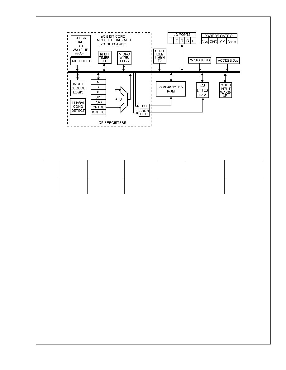
3.0 Block Diagram .............................................................................................................................................. 2
4.0 Ordering Information .................................................................................................................................... 2
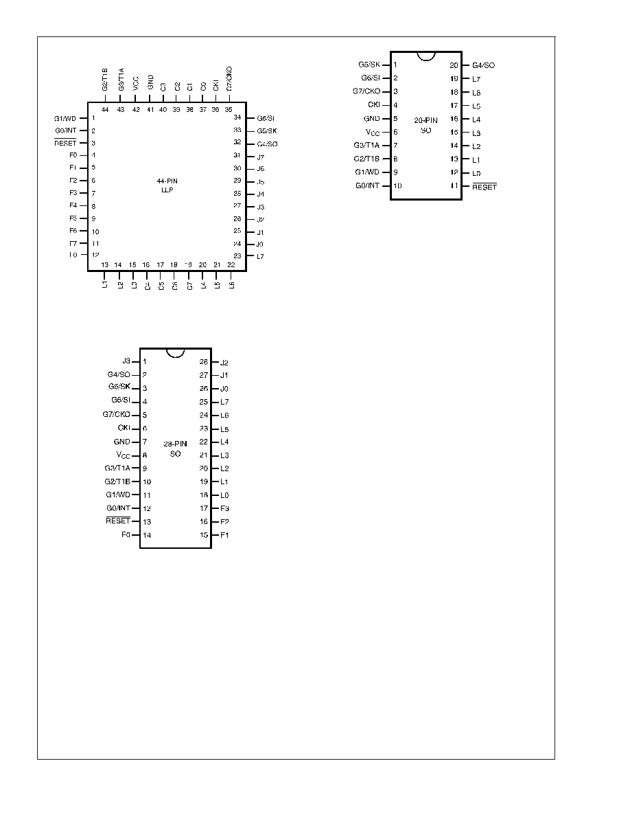
5.0 Connection Diagrams ................................................................................................................................... 5
6.0 Architectural Overview ................................................................................................................................. 7
6.1 EMI REDUCTION ...................................................................................................................................... 7
6.2 ARCHITECTURE
..................................................................................................................................... 7
6.3 INSTRUCTION SET
................................................................................................................................. 7
6.3.1 Key Instruction Set Features ............................................................................................................... 7
6.3.2 Single Byte/Single Cycle Code Execution
......................................................................................... 7
6.3.3 Many Single-Byte, Multi-Function Instructions .................................................................................... 7
6.3.4 Bit-Level Control .................................................................................................................................. 7
6.3.5 Register Set ......................................................................................................................................... 7
6.4 PACKAGING/PIN EFFICIENCY ................................................................................................................ 7
7.0 Absolute Maximum Ratings ......................................................................................................................... 8
8.0 Electrical Characteristics .............................................................................................................................. 8
9.0 Pin Descriptions ......................................................................................................................................... 11
10.0 Functional Description .............................................................................................................................. 13
10.1 CPU REGISTERS ................................................................................................................................. 13
10.2 PROGRAM MEMORY ........................................................................................................................... 14
10.3 DATA MEMORY .................................................................................................................................... 14
10.4 OPTION REGISTER ............................................................................................................................. 14
10.5 RESET ................................................................................................................................................... 15
10.5.1 External Reset ................................................................................................................................. 15
10.5.2 On-Chip Power-On Reset ................................................................................................................ 15
10.6 OSCILLATOR CIRCUITS ...................................................................................................................... 16
10.6.1 Crystal Oscillator .............................................................................................................................. 16
10.6.2 R/C Oscillator ................................................................................................................................... 16
10.6.3 External Oscillator ............................................................................................................................ 17
10.6.4 Clock Prescaler ................................................................................................................................ 17
10.7 CONTROL REGISTERS ....................................................................................................................... 18
10.7.1 CNTRL Register (Address X'00EE) ................................................................................................. 18
10.7.2 PSW Register (Address X'00EF) ..................................................................................................... 18
10.7.3 ICNTRL Register (Address X'00E8) ................................................................................................ 18
10.7.4 ITMR Register (Address X'00CF) .................................................................................................... 18
11.0 Timers ....................................................................................................................................................... 18
11.1 TIMER T0 (IDLE TIMER) ....................................................................................................................... 18
11.1.1 ITMR Register .................................................................................................................................. 19
11.2 TIMER T1 .............................................................................................................................................. 19
11.3 MODE 1. PROCESSOR INDEPENDENT PWM MODE ....................................................................... 19
11.4 MODE 2. EXTERNAL EVENT COUNTER MODE ................................................................................ 19
11.5 MODE 3. INPUT CAPTURE MODE ...................................................................................................... 21
11.6 TIMER CONTROL FLAGS .................................................................................................................... 22
12.0 Power Save Modes .................................................................................................................................. 22
12.1 HALT MODE .......................................................................................................................................... 22
12.2 IDLE MODE ........................................................................................................................................... 23
12.3 MULTI-INPUT WAKE-UP ...................................................................................................................... 24
13.0 Interrupts .................................................................................................................................................. 25
13.1 INTRODUCTION ................................................................................................................................... 25
13.2 MASKABLE INTERRUPTS ................................................................................................................... 26
13.3 VIS INSTRUCTION ............................................................................................................................... 27
13.3.1 VIS Execution .................................................................................................................................. 28
13.4 NON-MASKABLE INTERRUPT ............................................................................................................ 29
13.4.1 Pending Flag .................................................................................................................................... 29
13.4.2 Software Trap .................................................................................................................................. 29
13.4.2.1 Programming Example: External Interrupt ................................................................................. 30
13.5 PORT C AND PORT L INTERRUPTS .................................................................................................. 31
13.6 INTERRUPT SUMMARY ....................................................................................................................... 31
14.0 WATCHDOG/Clock Monitor ..................................................................................................................... 31
14.1 CLOCK MONITOR ................................................................................................................................ 32
14.2 WATCHDOG/CLOCK MONITOR OPERATION .................................................................................... 32
COP8T
AB5/T
AC5
www.national.com
3

Table of Contents
(Continued)
14.3 WATCHDOG AND CLOCK MONITOR SUMMARY .............................................................................. 32
14.4 DETECTION OF ILLEGAL CONDITIONS ............................................................................................ 33
15.0 MICROWIRE/PLUS .................................................................................................................................. 33
15.1 MICROWIRE/PLUS OPERATION ......................................................................................................... 33
15.2 MICROWIRE/PLUS MASTER MODE OPERATION ............................................................................. 34
15.3 MICROWIRE/PLUS SLAVE MODE OPERATION ................................................................................ 34
15.4 ALTERNATE SK PHASE OPERATION AND SK IDLE POLARITY ...................................................... 34
16.0 ACCESS.Bus Interface ............................................................................................................................ 36
16.1 DATA TRANSACTIONS ........................................................................................................................ 36
16.1.1 Start and Stop .................................................................................................................................. 37
16.1.2 Acknowledge Cycle .......................................................................................................................... 37
16.1.3 Addressing Transfer Formats .......................................................................................................... 37
16.2 BUS ARBITRATION .............................................................................................................................. 37
16.3 POWER SAVE MODES ........................................................................................................................ 37
16.4 SDA AND SCL DRIVER CONFIGURATION ......................................................................................... 37
16.5 ACB SERIAL DATA REGISTER (ACBSDA) .......................................................................................... 38
16.6 ACB STATUS REGISTER (ACBST) ..................................................................................................... 38
16.7 ACB CONTROL STATUS REGISTER (ACBCST) ................................................................................ 38
16.8 ACB CONTROL 1 REGISTER (ACBCTL1) .......................................................................................... 38
16.9 ACB CONTROL REGISTER 2 (ACBCTL2) .......................................................................................... 39
16.10 ACB OWN ADDRESS REGISTER (ACBADDR) ................................................................................ 39
17.0 Memory Map ............................................................................................................................................ 39
18.0 Instruction Set .......................................................................................................................................... 40
18.1 INTRODUCTION ................................................................................................................................... 40
18.2 INSTRUCTION FEATURES .................................................................................................................. 40
18.3 ADDRESSING MODES ......................................................................................................................... 40
18.3.1 Operand Addressing Modes ............................................................................................................ 40
18.3.2 Tranfer-of-Control Addressing Modes .............................................................................................. 41
18.4 INSTRUCTION TYPES ......................................................................................................................... 42
18.4.1 Arithmetic Instructions ...................................................................................................................... 42
18.4.2 Transfer-of-Control Instructions ....................................................................................................... 42
18.4.3 Load and Exchange Instructions ..................................................................................................... 43
18.4.4 Logical Instructions .......................................................................................................................... 43
18.4.5 Accumulator Bit Manipulation Instructions ....................................................................................... 43
18.4.6 Stack Control Instructions ................................................................................................................ 43
18.4.7 Memory Bit Manipulation Instructions ............................................................................................. 43
18.4.8 Conditional Instructions ................................................................................................................... 43
18.4.9 No-Operation Instruction .................................................................................................................. 43
18.5 REGISTER AND SYMBOL DEFINITION .............................................................................................. 43
18.6 INSTRUCTION SET SUMMARY .......................................................................................................... 44
18.7 INSTRUCTION EXECUTION TIME ...................................................................................................... 45
19.0 Development Support
............................................................................................................................. 48
19.1 TOOLS ORDERING NUMBERS FOR THE COP8TA 2.5V FAMILY DEVICES ................................... 48
19.2 COP8 TOOLS OVERVIEW ................................................................................................................... 49
19.3 WHERE TO GET TOOLS ..................................................................................................................... 50
20.0 Revision History ....................................................................................................................................... 52
21.0 Physical Dimensions ................................................................................................................................ 53
COP8T
AB5/T
AC5
www.national.com
4