COP880C
Microcontrollers
General Description
The following part numbers are pin count and tempera-
ture variations of the COP880C: COP680C/COP681C/
COP682C/COP881C
/COP882C/COP980C/
COP981C/COP982C.
The COP880C devices are members of the COP8 microcon-
troller family. They are fully static parts, fabricated using
double-metal silicon gate microCMOS technology. This low
cost microcontroller is a complete microcomputer containing
all system timing, interrupt logic, ROM, RAM, and I/O nec-
essary to implement dedicated control functions in a variety
of applications. Features include an 8-bit memory mapped
architecture, MICROWIRE/PLUS
TM
serial I/O, a 16-bit timer/
counter with capture register and a multi-sourced interrupt.
Each I/O pin has software selectable options to adapt the
device to the specific application. The part operates over a
voltage range of 2.5 to 6.0V. High throughput is achieved
with an efficient, regular instruction set operating at a 1
microsecond per instruction rate.
Key Features
n
-- 16-bit multi-function timer supporting
-- PWM mode
-- External event counter mode
-- Input capture mode
n
4 kbytes of ROM
n
128 bytes of RAM
I/O Features
n
Memory mapped I/O
n
Software selectable I/O options (TRI-STATE
Æ
, Push-Pull,
Weak Pull-Up Input, High Impedance Input)
n
High current outputs (8 pins)
n
Schmitt trigger inputs on Port G
n
MICROWIRE PLUS serial I/O
n
Packages:
-- 20 DIP/SO with 16 I/O pins
-- 28 DIP/SO with 24 I/O pins
-- 40 DIP, 36 I/O pins
-- 44 PLCC, 36 I/O pins
CPU/Instruction Set Features
n
1 µs instruction cycle time
n
Three multi-source interrupts servicing
-- External interrupt with selectable edge
-- Timer interrupt
-- Software interrupt
n
Versatile and easy to use instruction set
n
8-bit Stack Pointer (SP) -- stack in RAM
n
Two 8-bit Register Indirect Data Memory Pointers
(B and X)
Fully Static CMOS
n
Low current drain (typically
<
1 µA)
n
Single supply operation: 2.5V to 6.0V
n
Temperature ranges: 0∞C to 70∞C, -40∞C to +85∞C,
-55∞C to +125∞C.
Development Support
n
Emulation and OTP devices
n
Real time emulation and full program debug offered by
MetaLink's development system
TRI-STATE
Æ
is a registered trademark of National Semiconductor Corporation.
COPS
TM
, HPC
TM
, MICROWIRE
TM
and MICROWIRE/PLUS
TM
are trademarks of National Semiconductor Corporation.
iceMASTER
TM
is a trademark of MetaLink Corporation.
PC-XT
Æ
and PC-AT
Æ
are registered trademarks of International Business Machines Corporation.
August 1996
COP880C
Microcontrollers
© 2001 National Semiconductor Corporation
DS010802
www.national.com
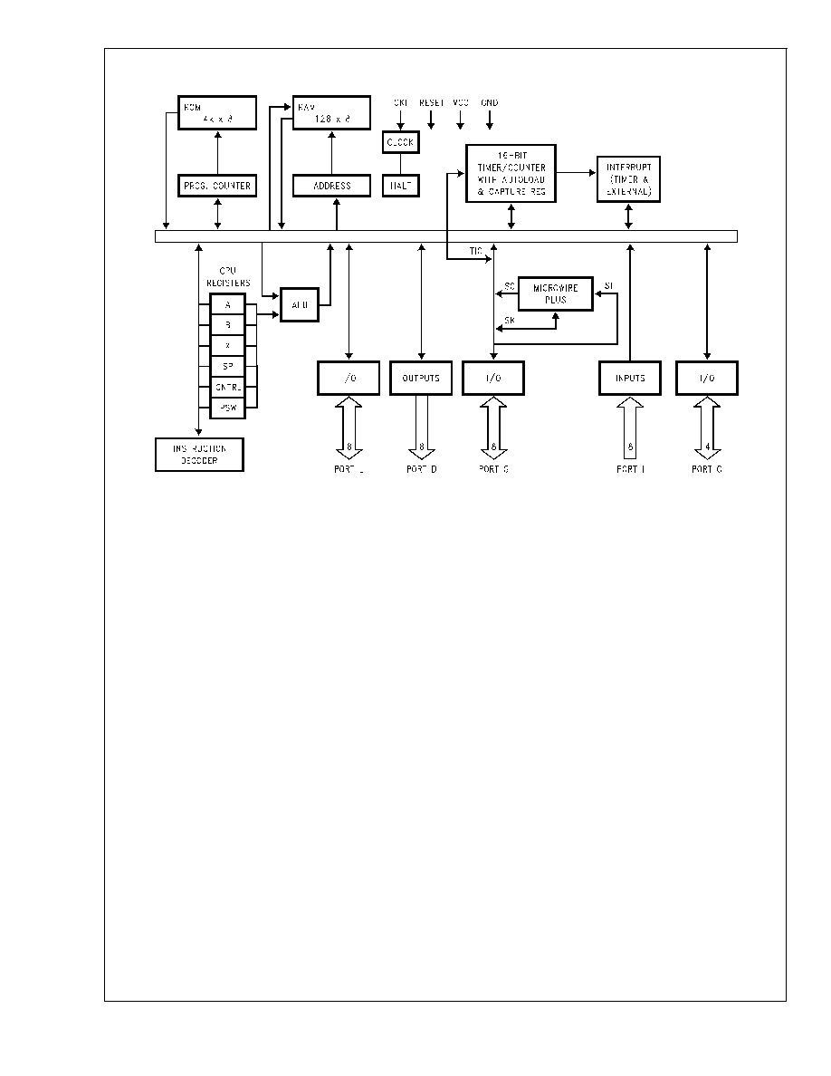
Block Diagram
DS010802-1
FIGURE 1.
COP880C
www.national.com
2
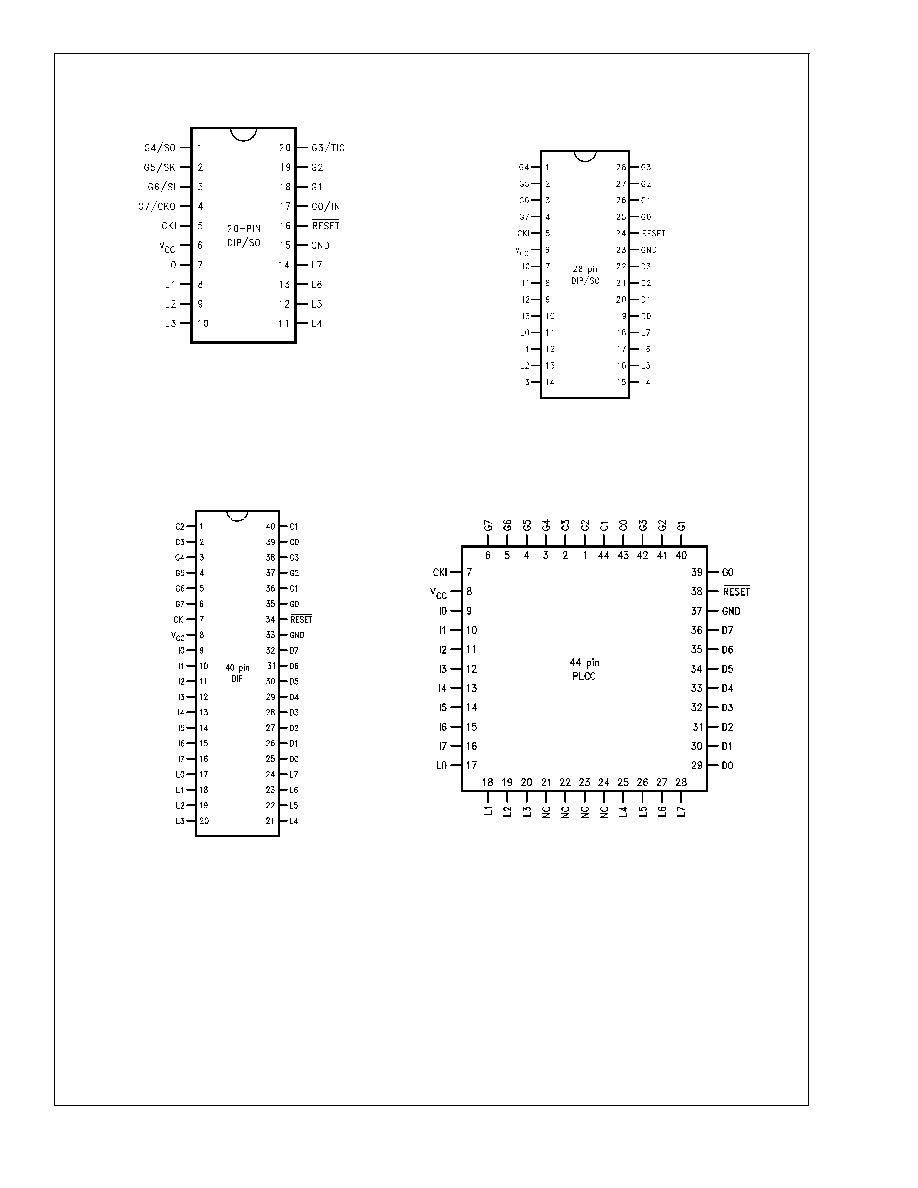
Connection Diagrams
Dual-In-Line Package
DS010802-23
Top View
Order Number COP882C-XXX/N, COP982C-XXX/N,
COP882C-XXX/WM, COP982C-XXX/WM,
COP982C-XXX/N or COP982CH-XXX/WM
Dual-In-Line Package (N)
and 28 Wide SO (WM)
DS010802-5
Top View
Order Number COP881C-XXX/N, COP981C-XXX/N,
COP881C-XXX/WM, COP981C-XXX/WM,
COP981CH-XXX/N or COP981CH-XXX/WM
Dual-In-Line Package
DS010802-4
Top View
Order Number COP680C-XXX/N, COP880C-XXX/N,
COP980C-XXX/N or COP980CH-XXX/N
Plastic Chip Carrier
DS010802-3
Top View
Order Number COP680C-XXX/V, COP880C-XXX/V,
COP980C-XXX/V or COP980CH-XXX/V
FIGURE 2. Connection Diagrams
COP880C
www.national.com
3
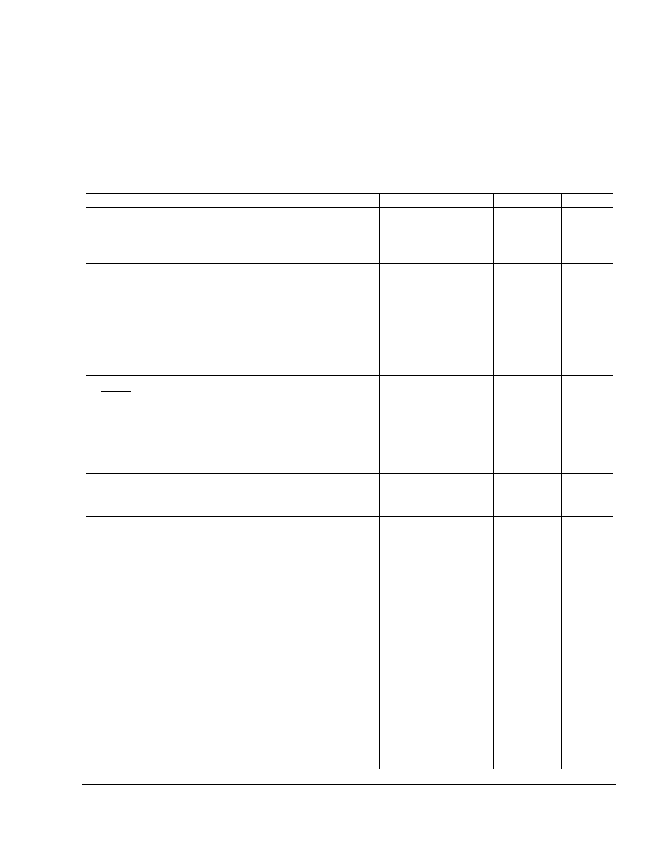
COP980C/COP981C/COP982C
Absolute Maximum Ratings
(Note 1)
If Military/Aerospace specified devices are required,
please contact the National Semiconductor Sales Office/
Distributors for availability and specifications.
Supply Voltage (V
CC
)
7V
Voltage at any Pin
-0.3V to V
CC
+ 0.3V
Total Current into V
CC
Pin (Source)
50 mA
Total Current out of GND Pin (Sink)
60 mA
Storage Temperature Range
-65∞C to +140∞C
Note 1: Absolute maximum ratings indicate limits beyond which damage to
the device may occur. DC and AC electrical specifications are not ensured
when operating the device at absolute maximum ratings.
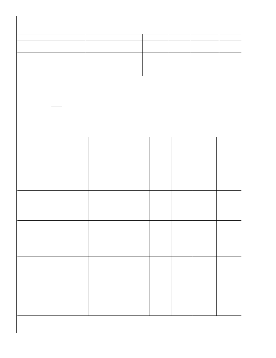
DC Electrical Characteristics
COP98xC; 0∞C
T
A
+70∞C unless otherwise specified
Parameter
Condition
Min
Typ
Max
Units
Operating Voltage
98XC
2.3
4.0
V
98XCH
4.0
6.0
V
Power Supply Ripple (Note 2)
Peak to Peak
0.1 V
CC
V
Supply Current
CKI = 10 MHz
V
CC
= 6V, tc = 1 µs
6.0
mA
CKI = 4 MHz
V
CC
= 6V, tc = 2.5 µs
4.4
mA
CKI = 4 MHz
V
CC
= 4.0V, tc = 2.5 µs
2.2
mA
CKI = 1 MHz
V
CC
= 4.0V, tc = 10 µs
1.4
mA
(Note 3)
HALT Current
V
CC
= 6V, CKI = 0 MHz
<
0.7
8
µA
(Note 4)
V
CC
= 4.0V, CKI = 0 MHz
<
0.4
5
µA
Input Levels
RESET, CKI
Logic High
0.9 V
CC
V
Logic Low
0.1 V
CC
V
All Other Inputs
Logic High
0.7 V
CC
V
Logic Low
0.2 V
CC
V
Hi-Z Input Leakage
V
CC
= 6.0V
-1.0
+1.0
µA
Input Pullup Current
V
CC
= 6.0V, V
IN
= 0V
-40
-250
µA
G Port Input Hysteresis
0.35 V
CC
V
Output Current Levels
D Outputs
Source
V
CC
= 4.5V, V
OH
= 3.8V
-0.4
mA
V
CC
= 2.3V, V
OH
= 1.6V
-0.2
mA
Sink
V
CC
= 4.5V, V
OL
= 1.0V
10
mA
V
CC
= 2.3V, V
OL
= 0.4V
2
mA
All Others
Source (Weak Pull-Up)
V
CC
= 4.5V, V
OH
= 3.2V
-10
-110
µA
V
CC
= 2.3V, V
OH
= 1.6V
-2.5
-33
µA
Source (Push-Pull Mode)
V
CC
= 4.5V, V
OH
= 3.8V
-0.4
mA
V
CC
= 2.3V, V
OH
= 1.6V
-0.2
Sink (Push-Pull Mode)
V
CC
= 4.5V, V
OL
= 0.4V
1.6
mA
V
CC
= 2.3V, V
OL
= 0.4V
0.7
TRI-STATE Leakage
V
CC
= 6.0V
-1.0
+1.0
µA
Allowable Sink/Source
Current Per Pin
D Outputs (Sink)
15
mA
All Others
3
mA
COP880C
www.national.com
4
DC Electrical Characteristics
(Continued)
COP98xC; 0∞C
T
A
+70∞C unless otherwise specified
Parameter
Condition
Min
Typ
Max
Units
Maximum Input Current (Note 5)
Without Latchup (Room Temp)
Room Temp
±
100
mA
RAM Retention Voltage, Vr
500 ns Rise and
(Note 6)
Fall Time (Min)
2.0
V
Input Capacitance
7
pF
Load Capacitance on D2
1000
pF
COP980C/COP981C/COP982C
Note 2: Rate of voltage change must be less than 0.5V/ms.
Note 3: Supply current is measured after running 2000 cycles with a square wave CKI input, CKO open, inputs at rails and outputs open.
Note 4: The HALT mode will stop CKI from oscillating in the RC and the Crystal configurations. Test conditions: All inputs tied to V
CC
, L, C and G ports TRI-STATE
and tied to ground, all outputs low and tied to ground.
Note 5: Pins G6 and RESET are designed with a high voltage input network for factory testing. These pins allow input voltages greater than V
CC
and the pins will
have sink current to V
CC
when biased at voltages greater than V
CC
(the pins do not have source current when biased at a voltage below V
CC
). The effective
resistance to V
CC
is 750
(typ). These two pins will not latch up. The voltage at the pins must be limited to less than 14V.
Note 6: To maintain RAM integrity, the voltage must not be dropped or raised instantaneously.
AC Electrical Characteristics
0∞C
T
A
+70∞C unless otherwise specified
Parameter
Condition
Min
Typ
Max
Units
Instruction Cycle Time (tc)
Crystal/Resonator or External
V
CC
4.0V
1
DC
µs
(Div-by 10)
2.3V
V
CC
4.0V
2.5
DC
µs
R/C Oscillator Mode
V
CC
4.0V
3
DC
µs
(Div-by 10)
2.3V
V
CC
4.0V
7.5
DC
µs
CKI Clock Duty Cycle (Note 7)
fr = Max
40
60
%
Rise Time (Note 7)
fr = 10 MHz Ext Clock
12
ns
Fall Time (Note 7)
fr = 10 MHz Ext Clock
8
ns
Inputs
t
SETUP
V
CC
4.0V
200
ns
2.3V
V
CC
4.0V
500
ns
t
HOLD
V
CC
4.0V
60
ns
2.3V
V
CC
4.0V
150
ns
Output Propagation Delay
C
L
= 100 pF, R
L
= 2.2 k
t
PD1
, t
PD0
SO, SK
V
CC
4.0V
0.7
µs
2.3V
V
CC
4.0V
1.75
µs
All Others
V
CC
4.0V
1
µs
2.3V
V
CC
4.0V
2.5
µs
MICROWIRE
TM
Setup Time (t
UWS)
20
ns
MICROWIRE Hold Time (t
UWH)
56
ns
MICROWIRE Output
Propagation Delay (t
UPD
)
220
ns
Input Pulse Width
Interrupt Input High Time
t
C
Interrupt Input Low Time
t
C
Timer Input High Time
t
C
Timer Input Low Time
t
C
Reset Pulse Width
1.0
µs
Note 7: Parameter characterized but not production tested.
COP880C
www.national.com
5