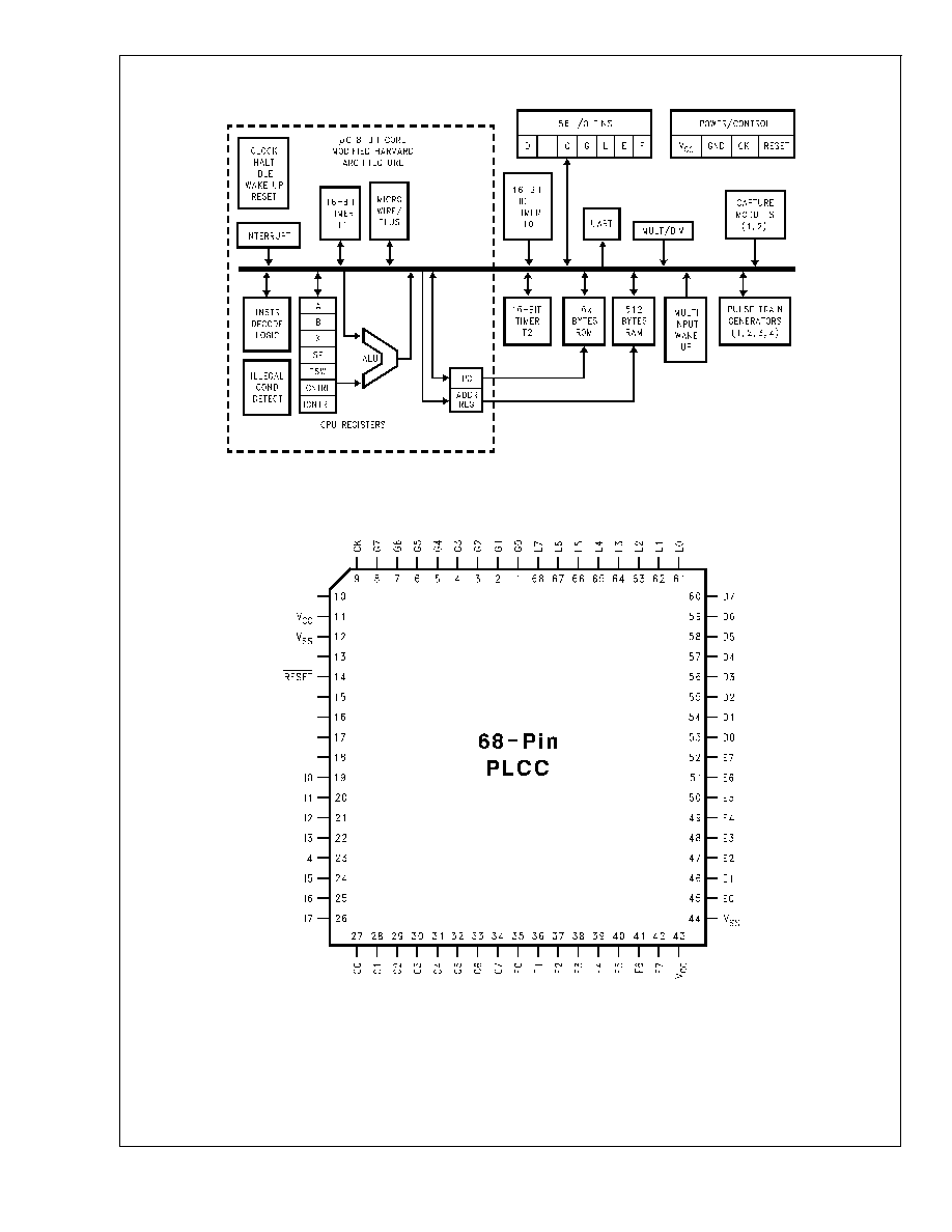
COP888GW
8-Bit Microcontroller with Pulse Train Generators and
Capture Modules
General Description
The COP888 family of microcontrollers uses an 8-bit single
chip core architecture fabricated with National Semiconduc-
tor's M
2
CMOS
TM
process technology. The COP888GW is a
member of this expandable 8-bit core processor family of
microcontrollers. It is a fully static part, fabricated using
double-metal silicon gate microCMOS technology.
Features include an 8-bit memory mapped architecture,
MICROWIRE/PLUS
TM
serial I/O, two 16-bit timer/counters
supporting three modes (Processor Independent PWM gen-
eration, External Event counter and Input Capture mode
capabilities), four independent 16-bit pulse train generators
with 16-bit prescalers, two independent 16-bit input capture
modules with 8-bit prescalers, multiply and divide functions,
full duplex UART, and two power savings modes (HALT and
IDLE), both with a multi-sourced wake up/interrupt capability.
This multi-sourced interrupt capability may also be used
independent of the HALT or IDLE modes.
Each I/O pin has software selectable configurations. The
devices operate over a voltage range of 2.5V≠6V. High
throughput is achieved with an efficient, regular instruction
set operating at a maximum of 1 µs per instruction rate. The
device has low EMI emissions. Low radiated emissions are
achieved by gradual turn-on output drivers and internal I
CC
filters on the chip logic and crystal oscillator. The device is
available in 68-pin PLCC package.
Key Features
n
Two 16-bit input capture modules with 8-bit prescalers
n
Four Pulse Train Generators with 16-bit prescalers
n
Full duplex UART
n
Two 16-bit timers, each with two 16-bit registers
supporting:
-- Processor independent PWM mode
-- External event counter mode
-- Input capture mode
n
Quiet design (low radiated emissions)
n
16 kbytes on-board ROM
n
512 bytes on-board RAM
Additional Peripheral Features
n
Idle Timer
n
Multi-Input Wake-Up (MIWU) with optional interrupts (8)
n
MICROWIRE/PLUS
TM
serial I/O
I/O Features
n
Memory mapped I/O
n
Software selectable I/O options ( TRI-STATE
Æ
Output,
Push-Pull Output, Weak Pull-Up Input, High Impedance
Input)
n
Schmitt trigger inputs on port G
n
Package:
68-pin PLCC
CPU/Instruction Set Features
n
1 µs instruction cycle time
n
Fourteen multi-source vectored interrupts servicing:
-- External Interrupt with selectable edge
-- Idle Timer T0
-- Two Timers (each with 2 interrupts)
-- MICROWIRE/PLUS
-- Multi-Input Wake-Up
-- Software Trap
-- UART (2)
-- Capture Timers
-- Counters (one vector for all four counters)
-- Default VIS (default interrupt)
n
Versatile and easy-to-use instruction set
n
8-bit Stack Pointer SP -- (stack in RAM)
n
Two 8-bit register indirect data memory pointers
(B and X)
Fully Static CMOS
n
Two power saving modes: HALT and IDLE
n
Low current drain (typically
<
1 µA)
n
Single supply operation: 2.5V≠5.5V
n
Temperature range: -40∞C to +85∞C
Development Support
n
Emulation and OTP device
n
Real time emulation and full program debug offered by
MetaLink's Development System
TRI-STATE
Æ
is a registered trademark of National Semiconductor Corporation.
M2CMOS
TM
, MICROWIRE/PLUS
TM
, COPS
TM
, MICROWIRE
TM
and WATCHDOG
TM
are trademarks of National Semiconductor Corporation.
IBM
Æ
, PC
Æ
, PC-AT
Æ
and PC/XT
Æ
are registered trademarks of International Business Machines Corporation.
iceMASTER
TM
is a trademark of MetaLink Corporation.
PRELIMINARY
August 1996
COP888GW
8-Bit
Microcontroller
with
Pulse
T
rain
Generators
and
Capture
Modules
© 2001 National Semiconductor Corporation
DS012065
www.national.com
Absolute Maximum Ratings
(Note 1)
SuppIy Voltage (V
CC
)
7V
Voltage at Any Pin
-0.3V to V
CC
+0.3V
Total Current into V
CC
Pin (Source)
100 mA
Total Current out of GND Pin (Sink)
110 mA
Storage Temperature Range
-65∞C to +150∞C
Note 1:
Absolute maximum ratings indicate limits beyond which damage to
the device may occur. DC and AC electrical specifications are not ensured
when operating the device at absolute maximum ratings.
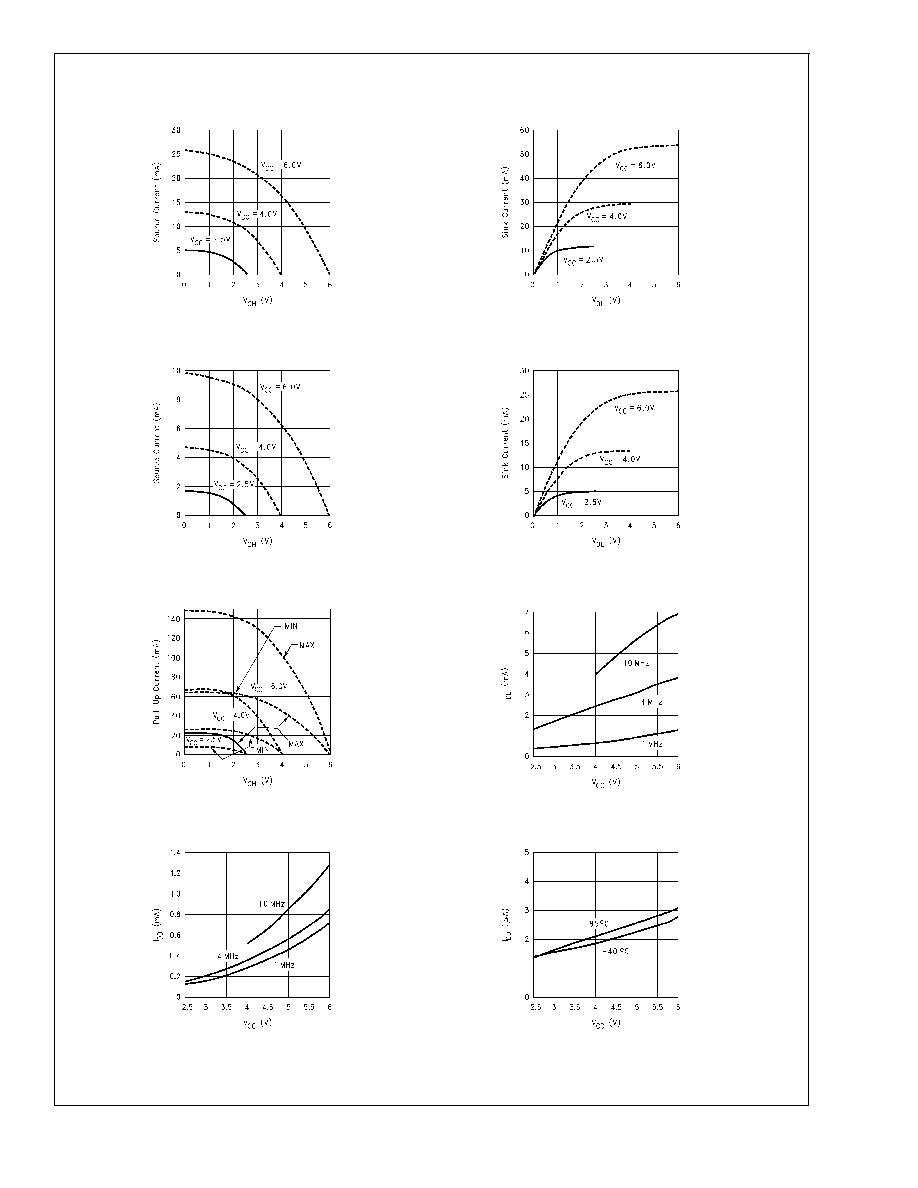
DC Electrical Characteristics
COP888GW: -40∞C
T
A
85∞C unless otherwise specified
Parameter
ConditIons
Min
Typ
Max
UnIts
Operating Voltage
2.5
6.0
V
Power Supply Ripple (Note 2)
Peak-to-Peak
0.1 V
CC
V
Supply Current (Note 3)
CKI = 10 MHz
V
CC
= 6V, t
c
= 1 µs
10
mA
CKI = 4 MHz
V
CC
= 2.5V, t
c
= 2.5 µs
1.7
mA
HALT Current (Note 4)
V
CC
= 6V, CKI = 0 MHz
<
1
10
µA
IDLE Current
CKI = 10 MHz
V
CC
= 6V
1.7
mA
CKI = 4 MHz
V
CC
= 2.5V
0.4
mA
Input Levels (V
IH
, V
IL
)
RESET , CKI
Logic High
0.8 V
CC
V
Logic Low
0.2 V
CC
V
All Other Inputs
Logic High
0.7 V
CC
V
Logic Low
0.2 V
CC
V
Hi-Z Input Leakage
V
CC
= 6V
-2
+2
µA
Input Pullup Current
V
CC
= 6V, V
IN
= 0V
-40
-250
µA
G Port Input Hysteresis
(Note 7)
0.05 V
CC
0.35 V
CC
V
Output Current Levels
D Outputs
Source
V
CC
= 4V, V
OH
= 3.3V
-0.4
mA
V
CC
= 2.5V, V
OH
= 1.8V
-0.2
mA
Sink
V
CC
= 4V, V
OL
= 1V
10
mA
V
CC
= 2.5V, V
OL
= 0.4V
2.0
mA
All Others
Source (Weak Pull-Up Mode)
V
CC
= 4V, V
OH
= 2.7V
-10
-100
µA
V
CC
= 2.5V, V
OH
= 1.8V
-2.5
-33
µA
Source (Push-Pull Mode)
V
CC
= 4V, V
OH
= 3.3V
-0.4
mA
V
CC
= 2.5V, V
OH
= 1.8V
-0.2
mA
Sink (Push-Pull Mode)
V
CC
= 4V, V
OL
= 0.4V
1.6
mA
V
CC
= 2.5V, V
OL
= 0.4V
0.7
mA
TRI-STATE Leakage
V
CC
= 6.0V
-2
+2
µA
Allowable Sink/Source
Current per Pin
D Outputs (Sink)
15
mA
All others
3
mA
Maximum Input Current
Room Temp
±
200
mA
without Latchup (Notes 5, 7)
RAM Retention Voltage, V
R
(Note 6)
500 ns Rise and Fall Time (min)
2
V
Input Capacitance
(Note 7)
7
pF
Load Capacitance on D2
(Note 7)
1000
pF
COP888GW
www.national.com
3
AC Electrical Characteristics
COP888GW: -40∞C
T
A
85∞C unless otherwise specified
Parameter
Conditions
Min
Typ
Max
Units
Instruction Cycle Time (t
c
)
Crystal, Resonator
2.5V
V
CC
<
4V
2.5
DC
µs
Ceramic
V
CC
4V
1.0
DC
µs
CKI Clock Duty Cycle (Note 6)
f = Max
40
60
%
Rise Time (Note 6)
f = 10 MHz Ext Clock
5
µs
Fall Time (Note 6)
f = 10 MHz Ext Clock
5
µs
Inputs
t
SETUP
V
CC
4V
200
ns
2.5V
V
CC
<
4V
500
ns
t
HOLD
V
CC
4V
60
ns
2.5V
V
CC
<
4V
150
ns
Output Propagation Delay (Note 9)
R
L
= 2.2k, C
L
= 100 pF
t
PD1
, t
PD0
SO, SK
V
CC
4V
0.7
µs
2.5V
V
CC
<
4V
1.8
µs
All Others
V
CC
4V
1
µs
2.5V
V
CC
<
4V
2.5
µs
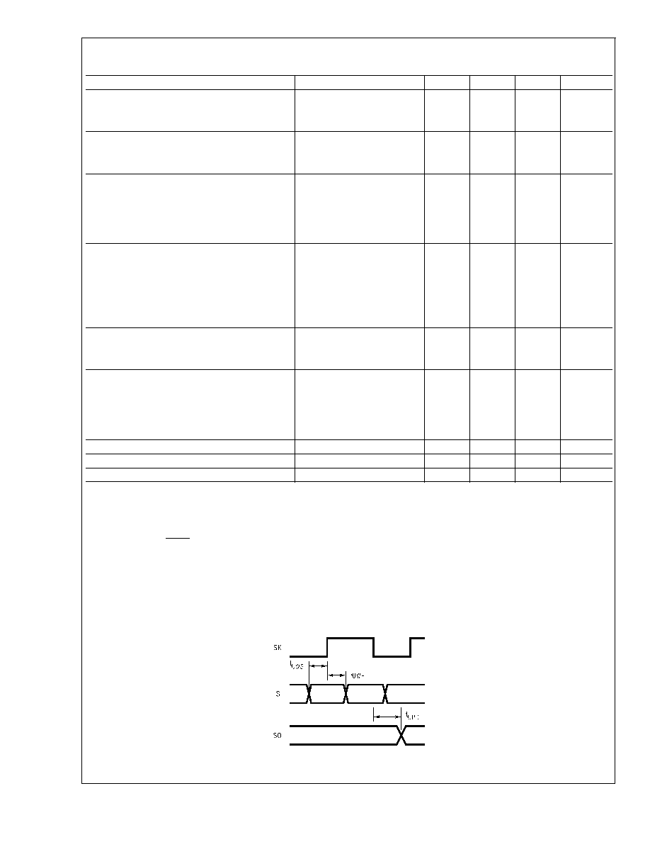
MICROWIRE
TM
Setup Time (t
UWS
) (Note 7)
V
CC
4V
20
ns
MICROWIRE Hold Time (t
UWH
) (Note 7)
V
CC
4V
56
ns
MICROWIRE Output Propagation Delay (t
UPD
)
V
CC
4V
220
ns
Input Pulse Width (Note 8)
Interrupt Input High Time
1
t
c
Interrupt Input Low Time
1
t
c
Timer 1, 2 Input High Time
1
t
c
Timer 1, 2 Input Low Time
1
t
c
Capture Timer High Time
1
CKI
Capture Timer Low Time
1
CKI
Reset Pause Width
1
t
c
Note 2: Maximum rate of voltage change to be defined.
Note 3: Supply current is measured after running 2000 cydes with a square wave CKI input, CKO open, inputs at rails and outputs open.
Note 4: The HALT mode will stop CKI from oscillatng. Test conditions: All inputs tied to V
CC
, L, C, E, F, and G port I/O's configured as outputs and programmed low
and not driving a load; D outputs programmed low and not driving a load. Parameter refers to HALT mode entered via setting bit 7 of the G Port data register. Part
will pull up CKI during HALT in crystal clock mode.
Note 5: Pins G6 and RESET are designed with a high voltage input network. These pins allow input voltages greater than V
CC
and the pins will have sink current
to V
CC
when biased at voltages greater than V
CC
(the pins do not have source current when biased at a voltage below V
CC
.) The effective resistance to V
CC
is 750
(typical). These two pins will not latch up. The voltage at the pins must be limited to less than 14 volts. WARNING: Voltages in excess of 14 volts will cause damage
to the pins. This warning excludes ESD transients.
Note 6: Condition and parameter valid only for part in HALT mode.
Note 7: Parameter characterized but not tested.
Note 8: t
c
= Instruction Cycle Time
Note 9: The output propagation delay is referenced to the end of the instruction cycle where the output change occurs.
DS012065-3
FIGURE 2. MICROWIRE/PLUS Timing
COP888GW
www.national.com
4