 | –≠–ª–µ–∫—Ç—Ä–æ–Ω–Ω—ã–π –∫–æ–º–ø–æ–Ω–µ–Ω—Ç: CP3SP33 | –°–∫–∞—á–∞—Ç—å:  PDF PDF  ZIP ZIP |
©2005 National Semiconductor Corporation
www.national.com
CP3SP33
Connec
t
iv
i
t
y Proc
e
s
s
o
r wi
t
h
C
a
c
h
e, DSP
,
a
nd Bluet
ooth, US
B
,
a
nd Dual CAN Inte
rfa
c
e
s
PRELIMINARY
September 2005
CP3SP33 Connectivity Processor with Cache, DSP, and
Bluetooth
Æ
, USB, and Dual CAN Interfaces
1.0
General Description
The CP3SP33 connectivity processor combines high per-
formance with the massive integration needed for embed-
ded Bluetooth applications. A powerful RISC core with 4K-
byte instruction cache and a Teak
Æ
DSP coprocessor pro-
vides high computing bandwidth, DMA-driven hardware
communications peripherals provide high I/O bandwidth,
and an external bus provides system expandability.
On-chip communications peripherals include: Bluetooth
Lower Link Controller, Universal Serial Bus (2.0) OTG node
and host controller, dual CAN, dual Microwire/Plus/SPI,
dual ACCESS.bus, quad UART, 10-bit A/D converter, and
telematics/audio codec. Additional on-chip peripherals in-
clude DMA controller, dual CVSD/PCM conversion module,
I
2
S and AAI digital audio bus interfaces, Timing and Watch-
dog Unit, dual Versatile Timer Unit, dual Multi-Function Tim-
er, and Multi-Input Wake-Up (MIWU) unit.
In addition to providing the features needed for the next gen-
eration of embedded Bluetooth products, the CP3SP33 is
backed up by the software resources that designers need
for rapid time-to-market, including an operating system,
Bluetooth protocol stack implementation, peripheral drivers,
reference designs, and an integrated development environ-
ment. Combined with an external program memory and a
Bluetooth radio transceiver such as National's LMX5252,
the CP3SP33 provides a complete Bluetooth system solu-
tion.
National Semiconductor offers a complete and industry-
proven application development environment for CP3SP33
applications, including the IAR Embedded Workbench,
iSYSTEM winIDEA and iC3000 Active Emulator, Bluetooth
Development Board, Bluetooth protocol stack, and applica-
tion examples.
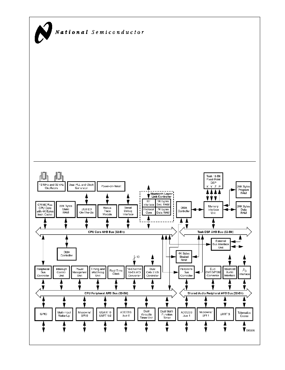
Block Diagram
Bluetooth is a registered trademark of Bluetooth SIG, Inc. and is used under license by National Semiconductor. Teak is a registered trademark of ParthusCeva, Inc.
TRI-STATE is a registered trademark of National Semiconductor Corporation.

www.national.com
2
CP
3SP
3
3
2.0
Features
CPU Features
Fully static RISC processor core, capable of operating
from 0 to 96 MHz with zero wait/hold state
Minimum 10.4 ns instruction cycle time with a 96-MHz in-
ternal clock frequency, based on a 12-MHz external input
4K-byte, 4-way set-associative instruction cache
69 independently vectored peripheral interrupts
DSP Features
Capable of operating up to 96 MHz
16-bit fixed-point arithmetic, dual-MAC architecture
32-bit interface to 4K-byte RAM shared with CPU
32-bit external bus interface
Bus master interface to audio peripherals and I/O
Memory
4K bytes CPU instruction cache
32K bytes CPU data RAM
4K bytes CPU/DSP shared RAM
24K bytes DSP program RAM
24K bytes DSP data RAM
8K bytes Bluetooth sequencer and data RAM
Addresses up to 32M bytes of external memory
Broad Range of Hardware Communications Peripher-
als
Bluetooth Lower Link Controller (LLC) including a shared
7K byte Bluetooth data RAM and 1K byte Bluetooth Se-
quencer RAM
Universal Serial Bus (USB) 2.0 On-The-Go
Audio/telematics codec with dual ADC inputs and high-
quality stereo DAC output
Two CAN interfaces with 15 message buffers conforming
to CAN specification 2.0B active
Two ACCESS.bus serial bus interfaces (I
2
C compatible)
Two 8/16-bit SPI, Microwire/Plus serial interfaces
I
2
S digital audio bus interface
Four Universal Asynchronous Receiver/Transmitter
(UART) channels, one channel has USART capability
Advanced Audio Interface (AAI) to connect to external 8/
13-bit PCM Codecs as well as to ISDN-Controllers
through the IOM-2 interface (slave only)
Two CVSD/PCM converters, for supporting two bidirec-
tional audio connections
External Bus Interface Shared Between CPU and DSP
16/32-bit data bus
23-bit address bus
3 programmable chip select outputs
Up to 32M bytes external memory
8-level write buffer
General-Purpose Hardware Peripherals
10-channel, 10-bit A/D Converter (ADC)
16-channel DMA controller
Dual 16-bit Multi-Function Timer (MFT)
Dual Versatile Timer Units (VTU), each with four inde-
pendent timers
Timing and Watchdog Unit
Extensive Power and Clock Management Support
Two Phase Locked Loops (PLL) for synthesizing inde-
pendent system and audio peripheral clocks
Two independent oscillators for Active mode (12 MHz)
and Power Save mode (32.768 kHz) clocks
Low-power modes (Power Save, Idle, and Halt) for slow-
ing or stopping clocks to optimize power consumption
while meeting application needs
Flexible I/O
Up to 64 general-purpose I/O pins (shared with on-chip
peripheral I/O)
Programmable I/O pin characteristics: TRI-STATE out-
put, push-pull output, weak pullup/pulldown input, high-
impedance input, high-speed drive capability
Schmitt triggers on general-purpose inputs
Multi-Input Wake-Up (MIWU) capability
Power Supply
I/O port operation at 3.0
≠
3.3V
Core logic operation at 1.8V
On-chip power-on reset
Temperature Range
-40∞C to +85∞C (Industrial)
Packages
FBGA-224, FBGA-144
Complete Development Environment
Pre-integrated hardware and software support for rapid
prototyping and production
Multi-file C source editor, source debugger, and project
manager
Comprehensive, integrated, one-stop technical support
Bluetooth Protocol Stack
Applications can interface to the high-level protocols or
directly to the low-level Host Controller Interface (HCI)
Transport layer support allows HCI command-based in-
terface over UART port
Baseband (Link Controller) hardware minimizes the
bandwidth demand on the CPU
Link Manager (LM)
Logical Link Control and Adaptation Protocol (L2CAP)
Service Discovery Protocol (SDP)
RFCOMM Serial Port Emulation Protocol
All packet types, piconet, and scatternet functionality
CP3SP33 Connectivity Processor Selection Guide
NSID
Speed
(MHz)
Temp. Range
I/Os
Package
Type
CP3SP33SMS
96
-40∞ to +85∞C
64
FBGA-224
CP3SP33SMR
96
-40∞ to +85∞C
36
FBGA-144

3
www.national.com
CP3
SP3
3
3.0
Device Overview
The CP3SP33 connectivity processor is an advanced mi-
crocomputer with system timing, interrupt logic, instruction
cache, data memory, and I/O ports included on-chip, mak-
ing it well-suited to a wide range of embedded applications.
The block diagram on page 1 shows the major on-chip com-
ponents of the CP3SP33.
3.1
CR16CPLUS CPU CORE
The CP3SP33 contains a CR16CPlus CPU core. This core
improves upon the performance of previous CP3000 devic-
es by adding a 4-Kbyte instruction cache and doubling the
CPU core data bus bandwidth. The cache greatly reduces
instruction-fetch bandwidth on the 32-bit system bus, which
leaves more bus bandwidth available for DMA-based I/O.
The cache moves the average execution rate closer to the
peak rate of one instruction per clock cycle, especially when
executing from off-chip program memory. The DMA control-
ler provides efficient sharing of the CPU core bus between
the CPU and high-bandwidth peripherals such as wired and
wireless communication interfaces.
For information on the instruction set architecture, please
refer to the CR16C Programmer's Reference Manual (doc-
ument number 424521772-101, which may be downloaded
from National's web site at http://www.national.com).
3.2
TEAK DSP CORE
The Teak 16-bit fixed-point DSP core is designed for low-
power, high-speed digital signal processing applications, in-
cluding acoustic echo cancellation, noise reduction, and
MP3/WMA decoding. It features a four-bus, dual-MAC, en-
hanced Harvard architecture. The DSP has 24K bytes of
dedicated program RAM, 24K bytes of data RAM, and a 4K-
byte RAM shared with the CPU. The DSP has a bus master
interface to the 4K-byte shared RAM and an external mem-
ory bus. It also has a bus master interface to a shared audio
peripheral bus. The DSP is slave on the CPU peripheral
bus, for downloading software to the program RAM.
The DSP has its own DMA controller for I/O and memory ac-
cess.
3.3
AMBA BUS ARCHITECTURE
The CPU and DSP core buses implement AMBA-compati-
ble AHB high-performance 32-bit buses with bursting and
split transactions. The CPU peripheral bus and CPU/DSP
shared audio peripheral bus implement AMBA-compatible
32-bit APB buses. The CPU and DSP buses operate at in-
dependent rates up to 96 MHz. The APB buses operate at
a rate which is a factor of 1, 2, or 4 slower than the CPU
AHB bus.
3.4
EXTERNAL BUS INTERFACE UNIT
The External Bus Interface Unit (EBIU) provides program-
mable timing, memory type, base address, size, and bus
width (8, 16, or 32 bits) for three regions of up to 32M bytes.
An 8-level write buffer releases the bus master to continue
execution without waiting for write cycles to complete.
3.5
MEMORY
The CP3SP33 devices support a uniform linear address
space. Three types of on-chip memory occupy specific re-
gions within this address space, along with any external
memory:
32K bytes of CPU RAM
4K bytes of CPU/DSP shared RAM
8K bytes of Bluetooth sequencer and data RAM
Up to 32M bytes of external memory
A non-volatile external program memory is used to store the
application program, Bluetooth protocol stack, and real-time
operating system.
The 32K bytes of CPU RAM are used for temporary storage
of data and for the program stack and interrupt stack. Read
and write operations can be byte-wide or word-wide, de-
pending on the instruction executed by the CPU.
3.6
BLUETOOTH LLC
The integrated hardware Bluetooth Lower Link Controller
(LLC) complies to the Bluetooth Specification Version 1.2
and integrates the following functions:
7K-byte dedicated Bluetooth data RAM
1K-byte dedicated Bluetooth sequencer RAM
Support of all Bluetooth 1.2 packet types and extended
Synchronous Connection-Oriented (eSCO) links
Support for fast frequency hopping of 1600 hops/s
Access code correlation and slot timing recovery circuit
Power Management Control Logic
BlueRF-compatible interface (mode 2/3) to connect with
National's LMX5252 and other RF transceiver chips
3.7
USB
The full-speed Universal Serial Bus (USB) node and host
controller is compatible with USB Specification 2.0 and USB
On-The-Go. It integrates the required USB transceiver, the
Serial Interface Engine (SIE), and USB endpoint FIFOs. A
total of seven endpoint pipes are supported: one bidirection-
al pipe for the mandatory control EP0 and an additional six
pipes for unidirectional endpoints to support USB interrupt,
bulk, and isochronous data transfers.
The on-chip USB transceiver features an integrated pullup
resistor on the D+ line to UVCC. This pullup resistor can be
switched in or out by the USB VBUS sense input (VBUS),
which eliminates the need for external components.
3.8
CAN INTERFACE
The two CAN modules support Full CAN 2.0B class, CAN
serial bus interfaces for applications that require a high-
speed (up to 1 Mbits per second) or a low-speed interface
with CAN bus master capability. The data transfer between
CAN and the CPU is established by 15 memory-mapped
message buffers, which can be individually configured as
receive or transmit buffers. An incoming message is filtered
by two masks, one for the first 14 message buffers and an-
other one for the 15th message buffer to provide a basic
CAN path. A priority decoder allows any buffer to have the
highest or lowest transmit priority. Remote transmission re-
quests can be processed automatically by automatic recon-
figuration to a receiver after transmission or by automated

www.national.com
4
CP
3SP
3
3
transmit scheduling upon reception. In addition, a 16-bit
time stamp counter supports real-time applications.
The CAN modules allow single-cycle byte or word read/
write access. A set of diagnostic features (such as loop-
back, listen only, and error identification) support the devel-
opment with the CAN modules and provide a sophisticated
error management tool.
The CAN receivers can trigger a wake-up condition out of
low-power modes through the Multi-Input Wake-Up unit.
3.9
AUDIO/TELEMATICS CODEC
The on-chip codec is designed for voice input and stereo
audio playback. It includes dual mono ADC channels oper-
ating at a sample rate of 8-24 kHz (125◊ oversampling clock
required). A stereo DAC operates at selected sample rates
from a 125◊ or 128◊ oversampling clock, driving two config-
urable, gain-programmable differential line driver outputs.
The DAC features click and pop reduction circuit, zero-
cross detector circuit, tone/compensation filter, sidetone in-
jection from ADC, and internal power management circuit.
The ADCs accept differential or single-ended analog micro-
phone inputs. The DAC employs fully differential signalling
for high PSRR and low crosstalk. DMA transfers are sup-
ported to allow for fast CPU-independent receive and trans-
mit.
3.10
CVSD/PCM CONVERSION MODULES
The two CVSD/PCM modules perform conversion between
CVSD data and PCM data, in which the CVSD encoding is
as defined in the Bluetooth specification and the PCM data
can be 8-bit µ-Law, 8-bit A-Law, or 13-bit to 16-bit Linear.
3.11
I
2
S DIGITAL AUDIO BUS
The Inter-IC Sound (I
2
S) interface is a synchronous serial
interface intended for the transfer of digital audio data. The
I
2
S interface can be configured as a master or a slave, and
it supports all three common data formats: I
2
S-mode, left-
justified, and right-justified. It has programmable word
length from 8 to 32 bits and programmable valid data reso-
lution from 8 to 24 bits.
3.12
ADVANCED AUDIO INTERFACE
The Advanced Audio Interface (AAI) provides a serial syn-
chronous, full-duplex interface to codecs and similar serial
devices. Transmit and receive paths operate asynchro-
nously with respect to each other. Each path uses three sig-
nals for communication: shift clock, frame synchronization,
and data.
When the receiver and transmitter use external shift clocks
and frame sync signals, the interface operates in its asyn-
chronous mode. Alternatively, the transmit and receive path
can share the same shift clock and frame sync signals for
synchronous mode operation.
3.13
ANALOG TO DIGITAL CONVERTER
This device contains a 10-channel, multiplexed input, suc-
cessive approximation, 10-bit Analog-to-Digital Converter. It
supports both single-ended and differential modes of oper-
ation.
The integrated 10-bit ADC provides the following features:
10-channel, multiplexed input
5 differential channels
Single-ended and differential external filtering capability
12-bit resolution; 10-bit accuracy
Sign bit
10-microsecond conversion time
External start trigger
Programmable start delay after start trigger
Poll or interrupt on conversion completion
The ADC provides several options for the voltage reference
source. The positive reference can be ADVCC (internal),
VREF, ADC0, or ADC1. The negative reference can be AD-
VCC (internal), ADC2, or ADC3.
Two specific analog channel selection modes are support-
ed. These are as follows:
Allow any specific channel to be selected at one time.
The A/D Converter performs the specific conversion re-
quested and stops.
Allow any differential channel pair to be selected at one
time. The A/D Converter performs the specific differential
conversion requested and stops.
In both single-ended and differential modes, there is the ca-
pability to connect the analog multiplexer output and A/D
converter input to external pins. This provides the ability to
externally connect a common filter/signal conditioning cir-
cuit for the A/D Converter.
3.14
QUAD UART
Four UART modules support a wide range of programmable
baud rates and data formats, parity generation, and several
error detection schemes. The baud rate is generated on-
chip, under software control. All UART modules support
DMA and hardware flow control. One module has USART
capability (synchronous mode) at speeds up to 921.6
kbaud. The UARTs offer a wake-up condition from the low-
power modes using the Multi-Input Wake-Up module.
3.15
MICROWIRE/SPI
The two Microwire/SPI (MWSPI) interface modules support
synchronous serial communications with other devices that
conform to Microwire or Serial Peripheral Interface (SPI)
specifications. It supports 8-bit and 16-bit data transfers.
The Microwire interfaces allows several devices to commu-
nicate over a single system consisting of four wires: serial
in, serial out, shift clock, and slave enable. At any given
time, the Microwire interfaces operate as a master or a
slave. The Microwire interfaces supports the full set of slave
select for multi-slave implementation.
In master mode, the shift clock is generated on-chip under
software control. In slave mode, a wake-up out of a low-
power mode may be triggered using the Multi-Input Wake-
Up module.

5
www.national.com
CP3
SP3
3
3.16
DUAL ACCESS.BUS INTERFACE
The two ACCESS.bus (ACB) interface modules support a
two-wire serial interface compatible with the ACCESS.bus
physical layer. It is also compatible with Intel's System Man-
agement Bus (SMBus) and Philips' I
2
C bus. The ACB mod-
ules can be configured as a bus master or slave, and they
can maintain bidirectional communications with both multi-
ple master and slave devices.
The ACCESS.bus receivers can trigger a wake-up condition
out of the low-power modes through the Multi-Input Wake-
Up module.
3.17
DUAL MULTI-FUNCTION TIMER
The two Multi-Function Timer (MFT) modules each contain
a pair of 16-bit timer/counter registers. Each timer/counter
unit can be configured to operate in any of the following
modes:
-- Processor-Independent Pulse Width Modulation
(PWM) mode: Generates pulses of a specified width
and duty cycle and provides a general-purpose timer/
counter.
-- Dual Input Capture mode: Measures the elapsed time
between occurrences of external event and provides
a general-purpose timer/counter.
-- Dual Independent Timer mode: Generates system
timing signals or counts occurrences of external
events.
-- Single Input Capture and Single Timer mode: Pro-
vides one external event counter and one system tim-
er.
3.18
VERSATILE TIMER UNITS
The two Versatile Timer Unit (VTU) modules each contain
four independent timer subsystems, which operate as a
dual 8-bit PWM configuration, a single 16-bit PWM timer, or
a 16-bit counter with two input capture channels. Each of
the timer subsystems offer an 8-bit clock prescaler to ac-
commodate a wide range of frequencies.
3.19
TIMING AND WATCHDOG MODULE
The Timing and Watchdog Module (TWM) contains a Real-
Time timer and a Watchdog unit. The Real-Time Clock Tim-
ing function can be used to generate periodic real-time
based system interrupts. The timer output is one of 16 in-
puts to the Multi-Input Wake-Up module which can be used
to exit from a low-power mode. The Watchdog unit is de-
signed to detect the application program getting stuck in an
infinite loop resulting in loss of program control or "runaway"
programs. When the watchdog triggers, it resets the device.
The TWM is clocked by the low-speed Slow Clock.
3.20
MULTI-INPUT WAKE-UP
The Multi-Input Wake-Up (MIWU) feature is used to return
(wake-up) the device from low-power modes to the active
mode. The 64-channel MIWU unit receives wake-up signals
from various internal and external sources. In addition to the
wake-up function, the MIWU unit can generate up to eight
interrupt requests. Each MIWU channel can be individually
programmed to activate one of the interrupt requests.
3.21
POWER MANAGEMENT
The Power Management Module (PMM) improves the effi-
ciency of the device by changing the operating mode and
power consumption to match the required level of activity.
The device can operate in any of four power modes:
-- Active: The device operates at full speed using the
high-frequency clock. All device functions are fully op-
erational.
-- Power Save: The device operates at reduced speed
using the Slow Clock. The CPU and some modules
can continue to operate at this low speed.
-- Idle: The device is inactive except for the Power Man-
agement Module and Timing and Watchdog Module,
which continue to operate using the Slow Clock.
-- Halt: The device is inactive but still retains its internal
state (RAM and register contents).
The PMM provides a mechanism to handle Bluetooth-spe-
cific power management modes, for optimizing power con-
sumption during special Bluetooth states, like Park, Page
Scan, Inquiry Scan, etc.
3.22
INPUT/OUTPUT PORTS
The device has 64 software-configurable I/O pins (36 in the
FBGA-144 package), organized into four ports called Port
E, Port F, Port G, and Port H. Each pin can be configured to
operate as a general-purpose input or general-purpose out-
put. In addition, many I/O pins can be configured to operate
as inputs or outputs for on-chip peripheral modules such as
the UARTs or timers.
The I/O pin characteristics are fully programmable. Each pin
can be configured to operate as a TRI-STATE output, push-
pull output, weak pullup/pulldown input, high-speed drive, or
high-impedance input.
3.23
CLOCK AND RESET MODULE
The Clock and Reset module generates a 12-MHz Main
Clock from an external crystal network or external clock in-
put. Main Clock may be used as a reference clock for two
PLL-based clock multipliers available for generating higher-
speed clocks.
Most modules operate from clocks derived from Main Clock
or a PLL clock. Modules on the CPU core AHB bus operate
from HCLK Clock, while modules on the peripheral APB
buses operate from PCLK Clock. PCLK Clock is generated
by dividing HCLK Clock by 1, 2, or 4. Some peripheral mod-
ules may use one of several auxiliary clocks, which also are
derived from Main Clock or a PLL clock using 12-bit pro-
grammable prescalers.
In Power-Save mode, HCLK Clock is driven by Slow Clock,
which is typically a 32.768 kHz signal generated from an ex-
ternal clock network or a prescaled Main Clock may be used
to eliminate the 32.768 kHz crystal network, for the most
cost-sensitive applications. In the most power-sensitive ap-
plications, operation from an external 32.768 kHz crystal
network allows the high-frequency oscillator and PLLs to be
shut down.