www.national.com
2
CP3UB1
7
Table of Contents
1.0
General Description . . . . . . . . . . . . . . . . . . . . . . . . . . 1
2.0
CPU Features . . . . . . . . . . . . . . . . . . . . . . . . . . . . . . . . 3
3.0
Device Overview . . . . . . . . . . . . . . . . . . . . . . . . . . . . . 4
3.1
CR16C CPU Core. . . . . . . . . . . . . . . . . . . . . . . . . . . . . . 4
3.2
Memory . . . . . . . . . . . . . . . . . . . . . . . . . . . . . . . . . . . . . . 4
3.3
Input/Output Ports. . . . . . . . . . . . . . . . . . . . . . . . . . . . . . 4
3.4
Bus Interface Unit . . . . . . . . . . . . . . . . . . . . . . . . . . . . . . 4
3.5
Interrupt Control Unit (ICU) . . . . . . . . . . . . . . . . . . . . . . . 4
3.6
USB. . . . . . . . . . . . . . . . . . . . . . . . . . . . . . . . . . . . . . . . . 4
3.7
Multi-Input Wake-up . . . . . . . . . . . . . . . . . . . . . . . . . . . . 4
3.8
Triple Clock and Reset . . . . . . . . . . . . . . . . . . . . . . . . . . 5
3.9
Power Management . . . . . . . . . . . . . . . . . . . . . . . . . . . . 5
3.10
Multi-Function Timer . . . . . . . . . . . . . . . . . . . . . . . . . . . . 5
3.11
Versatile Timer Unit . . . . . . . . . . . . . . . . . . . . . . . . . . . . 5
3.12
Timing and Watchdog Module . . . . . . . . . . . . . . . . . . . . 5
3.13
UART . . . . . . . . . . . . . . . . . . . . . . . . . . . . . . . . . . . . . . . 5
3.14
Microwire/SPI . . . . . . . . . . . . . . . . . . . . . . . . . . . . . . . . . 5
3.15
ACCESS.bus Interface . . . . . . . . . . . . . . . . . . . . . . . . . . 5
3.16
DMA CONTROLLER . . . . . . . . . . . . . . . . . . . . . . . . . . . 6
3.17
Advanced Audio interface . . . . . . . . . . . . . . . . . . . . . . . . 6
3.18
CVSD/PCM Conversion Module . . . . . . . . . . . . . . . . . . . 6
3.19
Serial Debug Interface . . . . . . . . . . . . . . . . . . . . . . . . . . 6
3.20
Development Support . . . . . . . . . . . . . . . . . . . . . . . . . . . 6
4.0
Device Pinouts . . . . . . . . . . . . . . . . . . . . . . . . . . . . . . . 7
4.1
Pin Description . . . . . . . . . . . . . . . . . . . . . . . . . . . . . . . 12
5.0
CPU Architecture . . . . . . . . . . . . . . . . . . . . . . . . . . . . 16
5.1
General-Purpose Registers . . . . . . . . . . . . . . . . . . . . . 16
5.2
Dedicated Address Registers . . . . . . . . . . . . . . . . . . . . 16
5.3
Processor Status Register (PSR) . . . . . . . . . . . . . . . . . 17
5.4
Configuration Register (CFG) . . . . . . . . . . . . . . . . . . . . 18
5.5
Addressing Modes . . . . . . . . . . . . . . . . . . . . . . . . . . . . 19
5.6
Stacks . . . . . . . . . . . . . . . . . . . . . . . . . . . . . . . . . . . . . . 20
5.7
Instruction Set . . . . . . . . . . . . . . . . . . . . . . . . . . . . . . . . 20
6.0
Memory . . . . . . . . . . . . . . . . . . . . . . . . . . . . . . . . . . . . 25
6.1
Operating Environment . . . . . . . . . . . . . . . . . . . . . . . . . 25
6.2
Bus Interface Unit (BIU) . . . . . . . . . . . . . . . . . . . . . . . . 25
6.3
Bus Cycles . . . . . . . . . . . . . . . . . . . . . . . . . . . . . . . . . . 26
6.4
BIU Control Registers . . . . . . . . . . . . . . . . . . . . . . . . . . 26
6.5
Wait and Hold States . . . . . . . . . . . . . . . . . . . . . . . . . . 28
7.0
System Configuration Registers . . . . . . . . . . . . . . . 29
7.1
Module Configuration Register (MCFG) . . . . . . . . . . . . 29
7.2
Module Status Register (MSTAT) . . . . . . . . . . . . . . . . . 29
8.0
Flash Memory . . . . . . . . . . . . . . . . . . . . . . . . . . . . . . 30
8.1
Flash Memory Protection . . . . . . . . . . . . . . . . . . . . . . . 30
8.2
Flash Memory Organization . . . . . . . . . . . . . . . . . . . . . 30
8.3
Flash Memory Operations. . . . . . . . . . . . . . . . . . . . . . . 31
8.4
Information Block Words. . . . . . . . . . . . . . . . . . . . . . . . 32
8.5
Flash Memory Interface Registers . . . . . . . . . . . . . . . . 34
9.0
DMA Controller . . . . . . . . . . . . . . . . . . . . . . . . . . . . . 40
9.1
Channel Assignment. . . . . . . . . . . . . . . . . . . . . . . . . . . 40
9.2
Transfer Types . . . . . . . . . . . . . . . . . . . . . . . . . . . . . . . 40
9.3
Operation Modes . . . . . . . . . . . . . . . . . . . . . . . . . . . . . 41
9.4
Software DMA Request . . . . . . . . . . . . . . . . . . . . . . . . 42
9.5
Debug Mode . . . . . . . . . . . . . . . . . . . . . . . . . . . . . . . . . 42
9.6
DMA Controller Register Set. . . . . . . . . . . . . . . . . . . . . 42
10.0
Interrupts . . . . . . . . . . . . . . . . . . . . . . . . . . . . . . . . . . 46
10.1
Non-Maskable Interrupts. . . . . . . . . . . . . . . . . . . . . . . . 46
10.2
Maskable Interrupts . . . . . . . . . . . . . . . . . . . . . . . . . . . 46
10.3
Interrupt Controller Registers . . . . . . . . . . . . . . . . . . . . 46
10.4
Maskable Interrupt Sources . . . . . . . . . . . . . . . . . . . . . 48
10.5
Nested Interrupts . . . . . . . . . . . . . . . . . . . . . . . . . . . . . 49
11.0
Triple Clock and Reset . . . . . . . . . . . . . . . . . . . . . . . 50
11.1
External Crystal Network . . . . . . . . . . . . . . . . . . . . . . . 51
11.2
Main Clock . . . . . . . . . . . . . . . . . . . . . . . . . . . . . . . . . . 51
11.3
Slow Clock . . . . . . . . . . . . . . . . . . . . . . . . . . . . . . . . . . 52
11.4
PLL Clock . . . . . . . . . . . . . . . . . . . . . . . . . . . . . . . . . . . 52
11.5
System Clock . . . . . . . . . . . . . . . . . . . . . . . . . . . . . . . . 52
11.6
Auxiliary Clocks. . . . . . . . . . . . . . . . . . . . . . . . . . . . . . . 52
11.7
Power-On Reset . . . . . . . . . . . . . . . . . . . . . . . . . . . . . . 52
11.8
External Reset . . . . . . . . . . . . . . . . . . . . . . . . . . . . . . . 52
11.9
Clock and Reset Registers . . . . . . . . . . . . . . . . . . . . . . 53
12.0
Power Management . . . . . . . . . . . . . . . . . . . . . . . . . . 55
12.1
Active Mode . . . . . . . . . . . . . . . . . . . . . . . . . . . . . . . . . 55
12.2
Power Save Mode. . . . . . . . . . . . . . . . . . . . . . . . . . . . . 55
12.3
Idle Mode . . . . . . . . . . . . . . . . . . . . . . . . . . . . . . . . . . . 55
12.4
Halt Mode . . . . . . . . . . . . . . . . . . . . . . . . . . . . . . . . . . . 55
12.5
Clock Control . . . . . . . . . . . . . . . . . . . . . . . . . . . . . . . . 56
12.6
Power Management Registers . . . . . . . . . . . . . . . . . . . 56
12.7
Switching Between Power Modes. . . . . . . . . . . . . . . . . 57
13.0
Multi-Input Wake-Up . . . . . . . . . . . . . . . . . . . . . . . . . 59
13.1
Multi-Input Wake-Up Registers . . . . . . . . . . . . . . . . . . . 59
13.2
Programming Procedures . . . . . . . . . . . . . . . . . . . . . . . 61
14.0
Input/Output Ports . . . . . . . . . . . . . . . . . . . . . . . . . . . 62
14.1
Port Registers . . . . . . . . . . . . . . . . . . . . . . . . . . . . . . . . 62
14.2
Open-Drain Operation. . . . . . . . . . . . . . . . . . . . . . . . . . 65
15.0
USB Controller . . . . . . . . . . . . . . . . . . . . . . . . . . . . . . 66
15.1
Functional States . . . . . . . . . . . . . . . . . . . . . . . . . . . . . . 66
15.2
Endpoint Operation . . . . . . . . . . . . . . . . . . . . . . . . . . . . 68
15.3
USB Controller Registers. . . . . . . . . . . . . . . . . . . . . . . . 70
15.4
Transceiver Interface . . . . . . . . . . . . . . . . . . . . . . . . . . . 85
16.0
Advanced Audio Interface . . . . . . . . . . . . . . . . . . . . . 86
16.1
Audio Interface Signals . . . . . . . . . . . . . . . . . . . . . . . . . 86
16.2
Audio Interface Modes . . . . . . . . . . . . . . . . . . . . . . . . . . 86
16.3
Bit Clock Generation . . . . . . . . . . . . . . . . . . . . . . . . . . . 89
16.4
Frame Clock Generation . . . . . . . . . . . . . . . . . . . . . . . . 89
16.5
Audio Interface Operation . . . . . . . . . . . . . . . . . . . . . . . 89
16.6
Communication Options. . . . . . . . . . . . . . . . . . . . . . . . . 91
16.7
Audio Interface Registers. . . . . . . . . . . . . . . . . . . . . . . . 94
17.0
CVSD/PCM Conversion Module . . . . . . . . . . . . . . . 101
17.1
Operation . . . . . . . . . . . . . . . . . . . . . . . . . . . . . . . . . . . 101
17.2
PCM Conversions . . . . . . . . . . . . . . . . . . . . . . . . . . . . 101
17.3
CVSD Conversion . . . . . . . . . . . . . . . . . . . . . . . . . . . . 102
17.4
PCM to CVSD Conversion. . . . . . . . . . . . . . . . . . . . . . 102
17.5
CVSD to PCM Conversion. . . . . . . . . . . . . . . . . . . . . . 102
17.6
Interrupt Generation. . . . . . . . . . . . . . . . . . . . . . . . . . . 102
17.7
DMA Support . . . . . . . . . . . . . . . . . . . . . . . . . . . . . . . . 102
17.8
Freeze . . . . . . . . . . . . . . . . . . . . . . . . . . . . . . . . . . . . . 103
17.9
CVSD/PCM Converter Registers . . . . . . . . . . . . . . . . . 103
18.0
UART Module . . . . . . . . . . . . . . . . . . . . . . . . . . . . . . 106
18.1
Functional Overview . . . . . . . . . . . . . . . . . . . . . . . . . . 106
18.2
UART Operation . . . . . . . . . . . . . . . . . . . . . . . . . . . . . 106
18.3
UART Registers . . . . . . . . . . . . . . . . . . . . . . . . . . . . . . 110
18.4
Baud Rate Calculations . . . . . . . . . . . . . . . . . . . . . . . . 114
19.0
Microwire/SPI Interface . . . . . . . . . . . . . . . . . . . . . . 116
19.1
Microwire Operation. . . . . . . . . . . . . . . . . . . . . . . . . . . 116
19.2
Master Mode . . . . . . . . . . . . . . . . . . . . . . . . . . . . . . . . 118
19.3
Slave Mode . . . . . . . . . . . . . . . . . . . . . . . . . . . . . . . . . 119
19.4
Interrupt Generation. . . . . . . . . . . . . . . . . . . . . . . . . . . 119
19.5
Microwire Interface Registers . . . . . . . . . . . . . . . . . . . 119
20.0
ACCESS.bus Interface . . . . . . . . . . . . . . . . . . . . . . . 122
20.1
ACB Protocol Overview . . . . . . . . . . . . . . . . . . . . . . . . 122
20.2
ACB Functional Description . . . . . . . . . . . . . . . . . . . . . 124
20.3
ACCESS.bus Interface Registers . . . . . . . . . . . . . . . . 126
20.4
Usage Hints . . . . . . . . . . . . . . . . . . . . . . . . . . . . . . . . . 130
21.0
Timing and Watchdog Module . . . . . . . . . . . . . . . . 131
21.1
TWM Structure. . . . . . . . . . . . . . . . . . . . . . . . . . . . . . . 131
21.2
Timer T0 Operation . . . . . . . . . . . . . . . . . . . . . . . . . . . 131
21.3
Watchdog Operation . . . . . . . . . . . . . . . . . . . . . . . . . . 132
21.4
TWM Registers . . . . . . . . . . . . . . . . . . . . . . . . . . . . . . 132
21.5
Watchdog Programming Procedure. . . . . . . . . . . . . . . 134
22.0
Multi-Function Timer . . . . . . . . . . . . . . . . . . . . . . . . 135
22.1
Timer Structure . . . . . . . . . . . . . . . . . . . . . . . . . . . . . . 135
22.2
Timer Operating Modes . . . . . . . . . . . . . . . . . . . . . . . . 136
22.3
Timer Interrupts . . . . . . . . . . . . . . . . . . . . . . . . . . . . . . 140
22.4
Timer I/O Functions . . . . . . . . . . . . . . . . . . . . . . . . . . . 140
22.5
Timer Registers . . . . . . . . . . . . . . . . . . . . . . . . . . . . . . 141
23.0
Versatile Timer Unit (VTU) . . . . . . . . . . . . . . . . . . . . 144
23.1
VTU Functional Description . . . . . . . . . . . . . . . . . . . . . 144
23.2
VTU Registers . . . . . . . . . . . . . . . . . . . . . . . . . . . . . . . 148
24.0
Register Map. . . . . . . . . . . . . . . . . . . . . . . . . . . . . . . 152
25.0
Register Bit Fields . . . . . . . . . . . . . . . . . . . . . . . . . . 162
26.0
Electrical Characteristics . . . . . . . . . . . . . . . . . . . . 172
26.1
Absolute Maximum Ratings . . . . . . . . . . . . . . . . . . . . . 172
26.2
DC Electrical Characteristics . . . . . . . . . . . . . . . . . . . . 172
26.3
USB Transceiver Electrical Characteristics . . . . . . . . . 173
26.4
Flash Memory On-Chip Programming . . . . . . . . . . . . . 174
26.5
Output Signal Levels . . . . . . . . . . . . . . . . . . . . . . . . . . 175
26.6
Clock and Reset Timing. . . . . . . . . . . . . . . . . . . . . . . . 175
26.7
UART Timing . . . . . . . . . . . . . . . . . . . . . . . . . . . . . . . . 177
26.8
I/O Port Timing. . . . . . . . . . . . . . . . . . . . . . . . . . . . . . . 178
26.9
Advanced Audio Interface (AAI) Timing. . . . . . . . . . . . 179
26.10
Microwire/SPI Timing . . . . . . . . . . . . . . . . . . . . . . . . . . 181
26.11
ACCESS.bus Timing . . . . . . . . . . . . . . . . . . . . . . . . . . 186
26.12
USB Port AC Characteristics . . . . . . . . . . . . . . . . . . . . 189
26.13
Multi-Function Timer (MFT) Timing . . . . . . . . . . . . . . . 189
26.14
Versatile Timing Unit (VTU) Timing . . . . . . . . . . . . . . . 190
26.15
External Bus Timing. . . . . . . . . . . . . . . . . . . . . . . . . . . 191
27.0
Revision History . . . . . . . . . . . . . . . . . . . . . . . . . . . . 196
28.0
Device Pinouts . . . . . . . . . . . . . . . . . . . . . . . . . . . . . 197
29.0
Physical Dimensions . . . . . . . . . . . . . . . . . . . . . . . . 199

www.national.com
4
CP3UB1
7
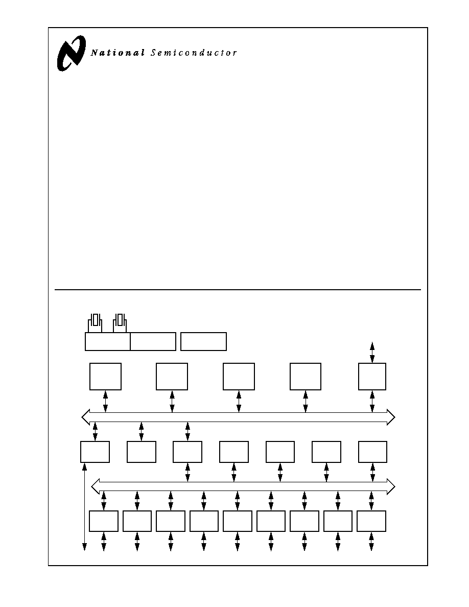
3.0
Device Overview
The CP3UB17 connectivity processor is a complete micro-
computers with all system timing, interrupt logic, program
memory, data memory, I/O ports included on-chip, making
them well-suited to a wide range of embedded applications.
The block diagram on page 1 shows the major on-chip com-
ponents of the CP3UB17.
3.1
CR16C CPU CORE
The CP3UB17 implements the CR16C CPU core module.
The high performance of the CPU core results from the im-
plementation of a pipelined architecture with a two-bytes-
per-cycle pipelined system bus. As a result, the CPU can
support a peak execution rate of one instruction per clock
cycle.
For more information, please refer to the CR16C Program-
mer's Reference Manual (document number 424521772-
101, which may be downloaded from National's web site at
http://www.national.com).
3.2
MEMORY
The CP3UB17 supports a uniform linear address space of
up to 16 megabytes. Three types of on-chip memory occupy
specific regions within this address space:
256K bytes of Flash program memory
8K bytes of Flash data memory
10K bytes of static RAM
Up to 8M bytes of external memory (100-pin devices )
The 256K bytes of Flash program memory are used to store
the application program and real-time operating system.
The Flash memory has security features to prevent uninten-
tional programming and to prevent unauthorized access to
the program code. This memory can be programmed with
an external programming unit or with the device installed in
the application system (in-system programming).
The 8K bytes of Flash data memory are used for non-vola-
tile storage of data entered by the end-user, such as config-
uration settings.
The 10K bytes of static RAM are used for temporary storage
of data and for the program stack and interrupt stack. Read
and write operations can be byte-wide or word-wide, de-
pending on the instruction executed by the CPU.
Up to 8M bytes of external memory can be added on an ex-
ternal bus. The external bus is only available on devices in
100-pin packages.
For Flash program and data memory, the device internally
generates the necessary voltages for programming. No ad-
ditional power supply is required.
3.3
INPUT/OUTPUT PORTS
The device has up to 37 software-configurable I/O pins, or-
ganized into five ports called Port B, Port C, Port G, Port H,
and Port I. Each pin can be configured to operate as a gen-
eral-purpose input or general-purpose output. In addition,
many I/O pins can be configured to operate as inputs or out-
puts for on-chip peripheral modules such as the UART, tim-
ers, or Microwire/SPI interface.
The I/O pin characteristics are fully programmable. Each pin
can be configured to operate as a TRI-STATE output, push-
pull output, weak pull-up input, or high-impedance input.
3.4
BUS INTERFACE UNIT
The Bus Interface Unit (BIU) controls access to internal/ex-
ternal memory and I/O. It determines the configured param-
eters for bus access (such as the number of wait states for
memory access) and issues the appropriate bus signals for
each requested access.
The BIU uses a set of control registers to determine how
many wait states and hold states are used when accessing
Flash program memory, and the I/O area (Port B and Port
C). At start-up, the configuration registers are set for slowest
possible memory access. To achieve fastest possible pro-
gram execution, appropriate values must be programmed.
These settings vary with the clock frequency and the type of
off-chip device being accessed.
3.5
INTERRUPT CONTROL UNIT (ICU)
The ICU receives interrupt requests from internal and exter-
nal sources and generates interrupts to the CPU. An inter-
rupt is an event that temporarily stops the normal flow of
program execution and causes a separate interrupt handler
to be executed. After the interrupt is serviced, CPU execu-
tion continues with the next instruction in the program fol-
lowing the point of interruption.
Interrupts from the timers, UART, Microwire/SPI interface,
and Multi-Input Wake-Up, are all maskable interrupts; they
can be enabled or disabled by software. There are 32 of
these maskable interrupts, assigned to 32 linear priority lev-
els.
The highest-priority interrupt is the Non-Maskable Interrupt
(NMI), which is generated by a signal received on the NMI
input pin.
3.6
USB
The USB node is a Universal Serial Bus (USB) Node con-
troller compatible with USB Specification, 1.0 and 1.1. It in-
tegrates the required USB transceiver, the Serial Interface
Engine (SIE), and USB endpoint FIFOs. A total of seven
endpoint pipes are supported: one bidirectional pipe for the
mandatory control EP0 and an additional six pipes for unidi-
rectional endpoints to support USB interrupt, bulk, and iso-
chronous data transfers.
3.7
MULTI-INPUT WAKE-UP
The Multi-Input Wake-Up (MIWU) module can be used for
either of two purposes: to provide inputs for waking up (ex-
iting) from the Halt, Idle, or Power Save mode; or to provide
general-purpose edge-triggered maskable interrupts from
external sources. This 16-channel module generates four
programmable interrupts to the CPU based on the signals
received on its 16 input channels. Channels can be individ-
ually enabled or disabled, and programmed to respond to
positive or negative edges.

5
www.national.com
CP3
UB17
3.8
TRIPLE CLOCK AND RESET
The Triple Clock and Reset module generates a high-speed
main System Clock from an external crystal network. It also
provides the main system reset signal and a power-on reset
function.
This module generates a slow System Clock (32.768 kHz)
from an optional external crystal network. The Slow Clock is
used for operating the device in power-save mode. The
32.768 kHz external crystal network is optional, because
the low speed System Clock can be derived from the high-
speed clock by a prescaler.
Also, two independent clocks divided down from the high
speed clock are available on output pins.
The Triple Clock and Reset module provides the clock sig-
nals required for the operation of the various CP3UB17 on-
chip modules. From external crystal networks, it generates
the Main Clock, which can be scaled up to 24 MHz from an
external 12 MHz input clock, and a 32.768 kHz secondary
System Clock. The 12 MHz external clock is primarily used
as the reference frequency for the on-chip PLL. Also the
clock for modules which require a fixed clock rate (e.g. the
PCM/CVSD transcoder) is generated through prescalers
from the 12 MHz clock. The PLL generates the input clock
for the USB node and may be used to drive the high-speed
System Clock through a prescaler. Alternatively, the high
speed System Clock can be derived directly from the 12
MHz Main Clock.
In addition, this module generates the device reset by using
reset input signals coming from an external reset and vari-
ous on-chip modules.
3.9
POWER MANAGEMENT
The Power Management Module (PMM) improves the effi-
ciency of the device by changing the operating mode and
power consumption to match the required level of activity.
The device can operate in any of four power modes:
Active--The device operates at full speed using the high-
frequency clock. All device functions are fully operation-
al.
Power Save--The device operates at reduced speed us-
ing the Slow Clock. The CPU and some modules can
continue to operate at this low speed.
Idle--The device is inactive except for the Power Man-
agement Module and Timing and Watchdog Module,
which continue to operate using the Slow Clock.
Halt--The device is inactive but still retains its internal
state (RAM and register contents).
3.10
MULTI-FUNCTION TIMER
The Multi-Function Timer (MFT) module contains a pair of
16-bit timer/counter registers. Each timer/counter unit can
be configured to operate in any of the following modes:
Processor-Independent Pulse Width Modulation (PWM)
mode--Generates pulses of a specified width and duty
cycle and provides a general-purpose timer/counter.
Dual Input Capture mode--Measures the elapsed time
between occurrences of external event and provides a
general-purpose timer/counter.
Dual Independent Timer mode--Generates system tim-
ing signals or counts occurrences of external events.
Single Input Capture and Single Timer mode--Provides
one external event counter and one system timer.
3.11
VERSATILE TIMER UNIT
The Versatile Timer Unit (VTU) module contains four inde-
pendent timer subsystems, each operating in either dual 8-
bit PWM configuration, as a single 16-bit PWM timer, or a
16-bit counter with two input capture channels. Each of the
four timer subsystems offer an 8-bit clock prescaler to ac-
commodate a wide range of frequencies.
3.12
TIMING AND WATCHDOG MODULE
The Timing and Watchdog Module (TWM) contains a Real-
Time timer and a Watchdog unit. The Real-Time Clock Tim-
ing function can be used to generate periodic real-time
based system interrupts. The timer output is one of 16 in-
puts to the Multi-Input-Wake-Up module which can be used
to exit from a power-saving mode. The Watchdog unit is de-
signed to detect the application program getting stuck in an
infinite loop resulting in loss of program control or "runaway"
programs. When the watchdog triggers, it resets the device.
The TWM is clocked by the low-speed System Clock.
3.13
UART
The UART supports a wide range of programmable baud
rates and data formats, parity generation, and several error
detection schemes. The baud rate is generated on-chip, un-
der software control.
The UART offers a wake-up condition from the power-save
mode using the Multi-Input Wake-Up module.
3.14
MICROWIRE/SPI
The Microwire/SPI (MWSPI) interface module supports syn-
chronous serial communications with other devices that
conform to Microwire or Serial Peripheral Interface (SPI)
specifications. It supports 8-bit and 16-bit data transfers.
The Microwire interface allows several devices to communi-
cate over a single system consisting of four wires: serial in,
serial out, shift clock, and slave enable. At any given time,
the Microwire interface operates as the master or a slave.
The Microwire interface supports the full set of slave select
for multi-slave implementation.
In master mode, the shift clock is generated on chip under
software control. In slave mode, a wake-up out of power-
save mode is triggered using the Multi-Input Wake-Up mod-
ule.
3.15
ACCESS.BUS INTERFACE
The ACCESS.bus interface module (ACB) is a two-wire se-
rial interface with the ACCESS.bus physical layer. It is also
compatible with Intel's System Management Bus (SMBus)
and Philips' I
2
C bus. The ACB module can be configured as
a bus master or slave, and can maintain bidirectional com-
munications with both multiple master and slave devices.
The ACCESS.bus receiver can trigger a wake-up condition
out of the low-power modes using the Multi-Input Wake-Up
module.