www.national.com
2
CP3UB2
6
Table of Contents
1.0
General Description . . . . . . . . . . . . . . . . . . . . . . . . . . 1
2.0
Features . . . . . . . . . . . . . . . . . . . . . . . . . . . . . . . . . . . . 3
3.0
Device Overview . . . . . . . . . . . . . . . . . . . . . . . . . . . . . 4
3.1
CR16C CPU Core . . . . . . . . . . . . . . . . . . . . . . . . . . . . . . . . . . . . . 4
3.2
Memory. . . . . . . . . . . . . . . . . . . . . . . . . . . . . . . . . . . . . . . . . . . . . . 4
3.3
Input/Output Ports . . . . . . . . . . . . . . . . . . . . . . . . . . . . . . . . . . . . . 4
3.4
Bus Interface Unit . . . . . . . . . . . . . . . . . . . . . . . . . . . . . . . . . . . . . . 4
3.5
Interrupt Control Unit (ICU). . . . . . . . . . . . . . . . . . . . . . . . . . . . . . . 4
3.6
Multi-Input Wake-up . . . . . . . . . . . . . . . . . . . . . . . . . . . . . . . . . . . . 4
3.7
USB . . . . . . . . . . . . . . . . . . . . . . . . . . . . . . . . . . . . . . . . . . . . . . . . 5
3.8
CAN Interface . . . . . . . . . . . . . . . . . . . . . . . . . . . . . . . . . . . . . . . . . 5
3.9
Quad UART . . . . . . . . . . . . . . . . . . . . . . . . . . . . . . . . . . . . . . . . . . 5
3.10
Advanced Audio interface. . . . . . . . . . . . . . . . . . . . . . . . . . . . . . . . 5
3.11
CVSD/PCM Conversion Module. . . . . . . . . . . . . . . . . . . . . . . . . . . 5
3.12
12-bit Analog to Digital Converter. . . . . . . . . . . . . . . . . . . . . . . . . . 5
3.13
Random Number Generator . . . . . . . . . . . . . . . . . . . . . . . . . . . . . . 5
3.14
Microwire/SPI . . . . . . . . . . . . . . . . . . . . . . . . . . . . . . . . . . . . . . . . . 6
3.15
ACCESS.bus Interface . . . . . . . . . . . . . . . . . . . . . . . . . . . . . . . . . . 6
3.16
Multi-Function Timer . . . . . . . . . . . . . . . . . . . . . . . . . . . . . . . . . . . . 6
3.17
Timing and Watchdog Module . . . . . . . . . . . . . . . . . . . . . . . . . . . . 6
3.18
Versatile Timer Unit . . . . . . . . . . . . . . . . . . . . . . . . . . . . . . . . . . . . 6
3.19
Triple Clock and Reset . . . . . . . . . . . . . . . . . . . . . . . . . . . . . . . . . . 6
3.20
Power Management . . . . . . . . . . . . . . . . . . . . . . . . . . . . . . . . . . . . 6
3.21
DMA Controller . . . . . . . . . . . . . . . . . . . . . . . . . . . . . . . . . . . . . . . . 7
3.22
Serial Debug Interface . . . . . . . . . . . . . . . . . . . . . . . . . . . . . . . . . . 7
3.23
Development Support. . . . . . . . . . . . . . . . . . . . . . . . . . . . . . . . . . . 7
4.0
Signal Descriptions . . . . . . . . . . . . . . . . . . . . . . . . . . . 8
5.0
CPU Architecture . . . . . . . . . . . . . . . . . . . . . . . . . . . . 15
5.1
General-Purpose Registers . . . . . . . . . . . . . . . . . . . . . . . . . . . . . 15
5.2
Dedicated Address Registers . . . . . . . . . . . . . . . . . . . . . . . . . . . . 15
5.3
Processor Status Register (PSR) . . . . . . . . . . . . . . . . . . . . . . . . . 16
5.4
Configuration Register (CFG) . . . . . . . . . . . . . . . . . . . . . . . . . . . . 17
5.5
Addressing Modes . . . . . . . . . . . . . . . . . . . . . . . . . . . . . . . . . . . . 18
5.6
Stacks. . . . . . . . . . . . . . . . . . . . . . . . . . . . . . . . . . . . . . . . . . . . . . 19
5.7
Instruction Set. . . . . . . . . . . . . . . . . . . . . . . . . . . . . . . . . . . . . . . . 19
6.0
Memory . . . . . . . . . . . . . . . . . . . . . . . . . . . . . . . . . . . . 24
6.1
Operating Environment. . . . . . . . . . . . . . . . . . . . . . . . . . . . . . . . . 24
6.2
Bus Interface Unit (BIU) . . . . . . . . . . . . . . . . . . . . . . . . . . . . . . . . 25
6.3
Bus Cycles . . . . . . . . . . . . . . . . . . . . . . . . . . . . . . . . . . . . . . . . . . 25
6.4
BIU Control Registers . . . . . . . . . . . . . . . . . . . . . . . . . . . . . . . . . . 25
6.5
Wait and Hold States . . . . . . . . . . . . . . . . . . . . . . . . . . . . . . . . . . 28
7.0
System Configuration Registers . . . . . . . . . . . . . . . 29
7.1
Module Configuration Register (MCFG) . . . . . . . . . . . . . . . . . . . . 29
7.2
Module Status Register (MSTAT). . . . . . . . . . . . . . . . . . . . . . . . . 30
7.3
Software Reset Register (SWRESET) . . . . . . . . . . . . . . . . . . . . . 30
8.0
Flash Memory . . . . . . . . . . . . . . . . . . . . . . . . . . . . . . 31
8.1
Flash Memory Protection . . . . . . . . . . . . . . . . . . . . . . . . . . . . . . . 31
8.2
Flash Memory Organization . . . . . . . . . . . . . . . . . . . . . . . . . . . . . 31
8.3
Flash Memory Operations . . . . . . . . . . . . . . . . . . . . . . . . . . . . . . 32
8.4
Information Block Words . . . . . . . . . . . . . . . . . . . . . . . . . . . . . . . 34
8.5
Flash Memory Interface Registers . . . . . . . . . . . . . . . . . . . . . . . . 35
9.0
DMA Controller . . . . . . . . . . . . . . . . . . . . . . . . . . . . . 41
9.1
Channel Assignment . . . . . . . . . . . . . . . . . . . . . . . . . . . . . . . . . . 41
9.2
Transfer Types . . . . . . . . . . . . . . . . . . . . . . . . . . . . . . . . . . . . . . . 41
9.3
Operation Modes . . . . . . . . . . . . . . . . . . . . . . . . . . . . . . . . . . . . . 42
9.4
Software DMA Request . . . . . . . . . . . . . . . . . . . . . . . . . . . . . . . . 43
9.5
Debug Mode . . . . . . . . . . . . . . . . . . . . . . . . . . . . . . . . . . . . . . . . . 43
9.6
DMA Controller Register Set . . . . . . . . . . . . . . . . . . . . . . . . . . . . 43
10.0
Interrupts . . . . . . . . . . . . . . . . . . . . . . . . . . . . . . . . . . 47
10.1
Non-Maskable Interrupts . . . . . . . . . . . . . . . . . . . . . . . . . . . . . . . 47
10.2
Maskable Interrupts . . . . . . . . . . . . . . . . . . . . . . . . . . . . . . . . . . . 47
10.3
Interrupt Controller Registers . . . . . . . . . . . . . . . . . . . . . . . . . . . . 47
10.4
Maskable Interrupt Sources . . . . . . . . . . . . . . . . . . . . . . . . . . . . . 50
10.5
Nested Interrupts . . . . . . . . . . . . . . . . . . . . . . . . . . . . . . . . . . . . . 50
11.0
Triple Clock and Reset . . . . . . . . . . . . . . . . . . . . . . . 51
11.1
External Crystal Network . . . . . . . . . . . . . . . . . . . . . . . . . . . . . . . 52
11.2
Main Clock . . . . . . . . . . . . . . . . . . . . . . . . . . . . . . . . . . . . . . . . . . 53
11.3
Slow Clock . . . . . . . . . . . . . . . . . . . . . . . . . . . . . . . . . . . . . . . . . . 53
11.4
PLL Clock . . . . . . . . . . . . . . . . . . . . . . . . . . . . . . . . . . . . . . . . . . . 53
11.5
System Clock . . . . . . . . . . . . . . . . . . . . . . . . . . . . . . . . . . . . . . . . 54
11.6
Auxiliary Clocks . . . . . . . . . . . . . . . . . . . . . . . . . . . . . . . . . . . . . . 54
11.7
Power-On Reset . . . . . . . . . . . . . . . . . . . . . . . . . . . . . . . . . . . . . . 54
11.8
External Reset . . . . . . . . . . . . . . . . . . . . . . . . . . . . . . . . . . . . . . . 54
11.9
Clock and Reset Registers . . . . . . . . . . . . . . . . . . . . . . . . . . . . . . 54
12.0
Power Management . . . . . . . . . . . . . . . . . . . . . . . . . . 56
12.1
Active Mode . . . . . . . . . . . . . . . . . . . . . . . . . . . . . . . . . . . . . . . . . 56
12.2
Power Save Mode . . . . . . . . . . . . . . . . . . . . . . . . . . . . . . . . . . . . 56
12.3
Idle Mode . . . . . . . . . . . . . . . . . . . . . . . . . . . . . . . . . . . . . . . . . . . 57
12.4
Halt Mode . . . . . . . . . . . . . . . . . . . . . . . . . . . . . . . . . . . . . . . . . . . 57
12.5
High-Frequency Oscillator and PLL Control . . . . . . . . . . . . . . . . . 57
12.6
Power Management Registers . . . . . . . . . . . . . . . . . . . . . . . . . . . 57
12.7
Switching Between Power Modes . . . . . . . . . . . . . . . . . . . . . . . . 59
13.0
Multi-Input Wake-Up . . . . . . . . . . . . . . . . . . . . . . . . . 61
13.1
Multi-Input Wake-Up Registers. . . . . . . . . . . . . . . . . . . . . . . . . . . 62
13.2
Programming Procedures. . . . . . . . . . . . . . . . . . . . . . . . . . . . . . . 66
14.0
Input/Output Ports . . . . . . . . . . . . . . . . . . . . . . . . . . . 67
14.1
Port Registers. . . . . . . . . . . . . . . . . . . . . . . . . . . . . . . . . . . . . . . . 67
14.2
Open-Drain Operation . . . . . . . . . . . . . . . . . . . . . . . . . . . . . . . . . 70
15.0
12-Bit Analog to Digital Converter . . . . . . . . . . . . . . 71
15.1
Functional Description . . . . . . . . . . . . . . . . . . . . . . . . . . . . . . . . . 71
15.2
Touchscreen Interface . . . . . . . . . . . . . . . . . . . . . . . . . . . . . . . . . 73
15.3
ADC Operation in Power-Saving Modes . . . . . . . . . . . . . . . . . . . 75
15.4
Freeze . . . . . . . . . . . . . . . . . . . . . . . . . . . . . . . . . . . . . . . . . . . . . 75
15.5
ADC Register Set . . . . . . . . . . . . . . . . . . . . . . . . . . . . . . . . . . . . . 75
16.0
Random Number Generator (RNG) . . . . . . . . . . . . . 80
16.1
Freeze . . . . . . . . . . . . . . . . . . . . . . . . . . . . . . . . . . . . . . . . . . . . . 80
16.2
Random Number Generator Register Set . . . . . . . . . . . . . . . . . . 81
17.0
USB Controller . . . . . . . . . . . . . . . . . . . . . . . . . . . . . . 82
17.1
Functional States . . . . . . . . . . . . . . . . . . . . . . . . . . . . . . . . . . . . . 82
17.2
Endpoint Operation . . . . . . . . . . . . . . . . . . . . . . . . . . . . . . . . . . . . 83
17.3
USB Controller Registers . . . . . . . . . . . . . . . . . . . . . . . . . . . . . . . 85
17.4
Transceiver Interface . . . . . . . . . . . . . . . . . . . . . . . . . . . . . . . . . 100
18.0
CAN Module . . . . . . . . . . . . . . . . . . . . . . . . . . . . . . . 101
18.1
Functional Description . . . . . . . . . . . . . . . . . . . . . . . . . . . . . . . . 101
18.2
Basic CAN Concepts . . . . . . . . . . . . . . . . . . . . . . . . . . . . . . . . . 102
18.3
Message Transfer . . . . . . . . . . . . . . . . . . . . . . . . . . . . . . . . . . . . 110
18.4
Acceptance Filtering . . . . . . . . . . . . . . . . . . . . . . . . . . . . . . . . . . 111
18.5
Receive Structure . . . . . . . . . . . . . . . . . . . . . . . . . . . . . . . . . . . . 112
18.6
Transmit Structure . . . . . . . . . . . . . . . . . . . . . . . . . . . . . . . . . . . 115
18.7
Interrupts. . . . . . . . . . . . . . . . . . . . . . . . . . . . . . . . . . . . . . . . . . . 117
18.8
Time Stamp Counter. . . . . . . . . . . . . . . . . . . . . . . . . . . . . . . . . . 118
18.9
Memory Organization . . . . . . . . . . . . . . . . . . . . . . . . . . . . . . . . . 119
18.10
CAN Controller Registers . . . . . . . . . . . . . . . . . . . . . . . . . . . . . . 120
18.11
System Start-Up and Multi-Input Wake-Up. . . . . . . . . . . . . . . . . 132
18.12
Usage Hint . . . . . . . . . . . . . . . . . . . . . . . . . . . . . . . . . . . . . . . . . 134
19.0
Advanced Audio Interface . . . . . . . . . . . . . . . . . . . . 135
19.1
Audio Interface Signals . . . . . . . . . . . . . . . . . . . . . . . . . . . . . . . . 135
19.2
Audio Interface Modes . . . . . . . . . . . . . . . . . . . . . . . . . . . . . . . . 135
19.3
Bit Clock Generation . . . . . . . . . . . . . . . . . . . . . . . . . . . . . . . . . . 138
19.4
Frame Clock Generation. . . . . . . . . . . . . . . . . . . . . . . . . . . . . . . 138
19.5
Audio Interface Operation . . . . . . . . . . . . . . . . . . . . . . . . . . . . . . 138
19.6
Communication Options . . . . . . . . . . . . . . . . . . . . . . . . . . . . . . . 140
19.7
Audio Interface Registers . . . . . . . . . . . . . . . . . . . . . . . . . . . . . . 143
20.0
CVSD/PCM Conversion Module . . . . . . . . . . . . . . . 150
20.1
Operation . . . . . . . . . . . . . . . . . . . . . . . . . . . . . . . . . . . . . . . . . . 150
20.2
PCM Conversions . . . . . . . . . . . . . . . . . . . . . . . . . . . . . . . . . . . . 150
20.3
CVSD Conversion. . . . . . . . . . . . . . . . . . . . . . . . . . . . . . . . . . . . 151
20.4
PCM to CVSD Conversion . . . . . . . . . . . . . . . . . . . . . . . . . . . . . 151
20.5
CVSD to PCM Conversion . . . . . . . . . . . . . . . . . . . . . . . . . . . . . 151
20.6
Interrupt Generation . . . . . . . . . . . . . . . . . . . . . . . . . . . . . . . . . . 151
20.7
DMA Support . . . . . . . . . . . . . . . . . . . . . . . . . . . . . . . . . . . . . . . 151
20.8
Freeze. . . . . . . . . . . . . . . . . . . . . . . . . . . . . . . . . . . . . . . . . . . . . 152
20.9
CVSD/PCM Converter Registers . . . . . . . . . . . . . . . . . . . . . . . . 152
21.0
UART Modules . . . . . . . . . . . . . . . . . . . . . . . . . . . . . 155
21.1
Functional Overview . . . . . . . . . . . . . . . . . . . . . . . . . . . . . . . . . . 155
21.2
UART Operation . . . . . . . . . . . . . . . . . . . . . . . . . . . . . . . . . . . . . 155
21.3
UART Registers . . . . . . . . . . . . . . . . . . . . . . . . . . . . . . . . . . . . . 160
21.4
Baud Rate Calculations . . . . . . . . . . . . . . . . . . . . . . . . . . . . . . . 164
22.0
Microwire/SPI Interface . . . . . . . . . . . . . . . . . . . . . . 167
22.1
Microwire Operation . . . . . . . . . . . . . . . . . . . . . . . . . . . . . . . . . . 167
22.2
Master Mode . . . . . . . . . . . . . . . . . . . . . . . . . . . . . . . . . . . . . . . . 169
22.3
Slave Mode . . . . . . . . . . . . . . . . . . . . . . . . . . . . . . . . . . . . . . . . . 170
22.4
Interrupt Generation . . . . . . . . . . . . . . . . . . . . . . . . . . . . . . . . . . 170
22.5
Microwire Interface Registers . . . . . . . . . . . . . . . . . . . . . . . . . . . 171
23.0
ACCESS.bus Interface . . . . . . . . . . . . . . . . . . . . . . . 173
23.1
ACB Protocol Overview . . . . . . . . . . . . . . . . . . . . . . . . . . . . . . . 173
23.2
ACB Functional Description . . . . . . . . . . . . . . . . . . . . . . . . . . . . 175
23.3
ACCESS.bus Interface Registers . . . . . . . . . . . . . . . . . . . . . . . . 177
23.4
Usage Hints . . . . . . . . . . . . . . . . . . . . . . . . . . . . . . . . . . . . . . . . 181
24.0
Timing and Watchdog Module . . . . . . . . . . . . . . . . 184
24.1
TWM Structure . . . . . . . . . . . . . . . . . . . . . . . . . . . . . . . . . . . . . . 184
24.2
Timer T0 Operation. . . . . . . . . . . . . . . . . . . . . . . . . . . . . . . . . . . 184
24.3
Watchdog Operation . . . . . . . . . . . . . . . . . . . . . . . . . . . . . . . . . . 185
24.4
TWM Registers . . . . . . . . . . . . . . . . . . . . . . . . . . . . . . . . . . . . . . 185
24.5
Watchdog Programming Procedure . . . . . . . . . . . . . . . . . . . . . . 187
25.0
Multi-Function Timer . . . . . . . . . . . . . . . . . . . . . . . . 188
25.1
Timer Structure . . . . . . . . . . . . . . . . . . . . . . . . . . . . . . . . . . . . . . 188
25.2
Timer Operating Modes . . . . . . . . . . . . . . . . . . . . . . . . . . . . . . . 189
25.3
Timer Interrupts . . . . . . . . . . . . . . . . . . . . . . . . . . . . . . . . . . . . . 194
25.4
Timer I/O Functions . . . . . . . . . . . . . . . . . . . . . . . . . . . . . . . . . . 194
25.5
Timer Registers . . . . . . . . . . . . . . . . . . . . . . . . . . . . . . . . . . . . . 195
26.0
Versatile Timer Unit (VTU) . . . . . . . . . . . . . . . . . . . . 198
26.1
VTU Functional Description . . . . . . . . . . . . . . . . . . . . . . . . . . . . 198
26.2
VTU Registers . . . . . . . . . . . . . . . . . . . . . . . . . . . . . . . . . . . . . . 202
27.0
Register Map. . . . . . . . . . . . . . . . . . . . . . . . . . . . . . . 206
28.0
Register Bit Fields . . . . . . . . . . . . . . . . . . . . . . . . . . 221
29.0
Electrical Characteristics . . . . . . . . . . . . . . . . . . . . 233
29.1
Absolute Maximum Ratings . . . . . . . . . . . . . . . . . . . . . . . . . . . . 233
29.2
DC Electrical Characteristics . . . . . . . . . . . . . . . . . . . . . . . . . . . 233
29.3
USB Transceiver Electrical Characteristics . . . . . . . . . . . . . . . . 235
29.4
ADC Electrical Characteristics . . . . . . . . . . . . . . . . . . . . . . . . . . 235
29.5
Flash Memory On-Chip Programming . . . . . . . . . . . . . . . . . . . . 236
29.6
Output Signal Levels. . . . . . . . . . . . . . . . . . . . . . . . . . . . . . . . . . 237
29.7
Clock and Reset Timing . . . . . . . . . . . . . . . . . . . . . . . . . . . . . . . 237
29.8
UART Timing . . . . . . . . . . . . . . . . . . . . . . . . . . . . . . . . . . . . . . . 239
29.9
I/O Port Timing . . . . . . . . . . . . . . . . . . . . . . . . . . . . . . . . . . . . . . 240
29.10
Advanced Audio Interface (AAI) Timing . . . . . . . . . . . . . . . . . . . 241
29.11
Microwire/SPI Timing . . . . . . . . . . . . . . . . . . . . . . . . . . . . . . . . . 243
29.12
ACCESS.bus Timing . . . . . . . . . . . . . . . . . . . . . . . . . . . . . . . . . 248
29.13
USB Port AC Characteristics . . . . . . . . . . . . . . . . . . . . . . . . . . . 251
29.14
Multi-Function Timer (MFT) Timing . . . . . . . . . . . . . . . . . . . . . . 251
29.15
Versatile Timing Unit (VTU) Timing . . . . . . . . . . . . . . . . . . . . . . 252
29.16
External Bus Timing . . . . . . . . . . . . . . . . . . . . . . . . . . . . . . . . . . 253
30.0
Pin Assignments . . . . . . . . . . . . . . . . . . . . . . . . . . . 259
30.1
LQFP-128 Package . . . . . . . . . . . . . . . . . . . . . . . . . . . . . . . . . . 259
30.2
LQFP-144 Package . . . . . . . . . . . . . . . . . . . . . . . . . . . . . . . . . . 262
31.0
Revision History . . . . . . . . . . . . . . . . . . . . . . . . . . . . 266
32.0
Physical Dimensions . . . . . . . . . . . . . . . . . . . . . . . . 267

www.national.com
4
CP3UB2
6
3.0
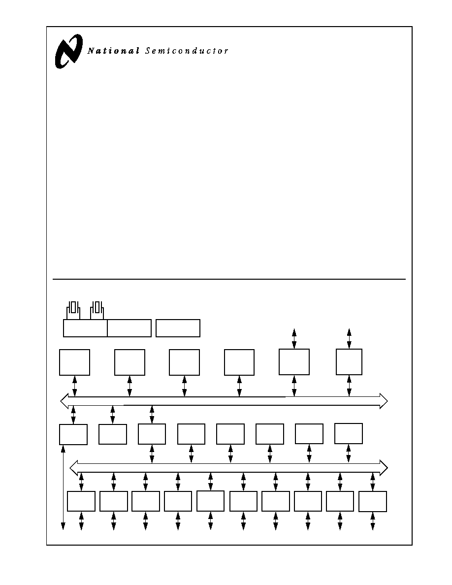
Device Overview
The CP3UB26 connectivity processor is a complete micro-
computer with all system timing, interrupt logic, program
memory, data memory, and I/O ports included on-chip, mak-
ing it well-suited to a wide range of embedded applications.
The block diagram on page 1 shows the major on-chip com-
ponents of the CP3UB26 devices.
3.1
CR16C CPU CORE
The CP3UB26 device implements the CR16C CPU core
module. The high performance of the CPU core results from
the implementation of a pipelined architecture with a two-
bytes-per-cycle pipelined system bus. As a result, the CPU
can support a peak execution rate of one instruction per
clock cycle.
For more information, please refer to the CR16C Program-
mer's Reference Manual (document number 424521772-
101, which may be downloaded from National's web site at
http://www.national.com).
3.2
MEMORY
The CP3UB26 devices support a uniform linear address
space of up to 16 megabytes. Three types of on-chip mem-
ory occupy specific regions within this address space, along
with any external memory:
256K bytes of Flash program memory
8K bytes of Flash data memory
32K bytes of static RAM
Up to 12M bytes of external memory (144-pin devices)
The 256K bytes of Flash program memory are used to store
the application program and real-time operating system.
The Flash memory has security features to prevent uninten-
tional programming and to prevent unauthorized access to
the program code. This memory can be programmed with
an external programming unit or with the device installed in
the application system (in-system programming).
The 8K bytes of Flash data memory are used for non-vola-
tile storage of data entered by the end-user, such as config-
uration settings.
The 32K bytes of static RAM are used for temporary storage
of data and for the program stack and interrupt stack. Read
and write operations can be byte-wide or word-wide, de-
pending on the instruction executed by the CPU.
Up to 12M bytes of external memory can be added on an
external bus. The external bus is only available on devices
in 144-pin packages.
For Flash program and data memory, the device internally
generates the necessary voltages for programming. No ad-
ditional power supply is required.
3.3
INPUT/OUTPUT PORTS
The device has up to 54 software-configurable I/O pins, or-
ganized into seven ports called Port B, Port C, Port E, Port
G, Port H, Port I, and Port J. Each pin can be configured to
operate as a general-purpose input or general-purpose out-
put. In addition, many I/O pins can be configured to operate
as inputs or outputs for on-chip peripheral modules such as
the UART, timers, or Microwire/SPI interface.
The I/O pin characteristics are fully programmable. Each pin
can be configured to operate as a TRI-STATE output, push-
pull output, weak pull-up input, or high-impedance input.
3.4
BUS INTERFACE UNIT
The Bus Interface Unit (BIU) controls access to internal/ex-
ternal memory and I/O. It determines the configured param-
eters for bus access (such as the number of wait states for
memory access) and issues the appropriate bus signals for
each requested access.
The BIU uses a set of control registers to determine how
many wait states and hold states are used when accessing
Flash program memory and the I/O area. At start-up, the
configuration registers are set for slowest possible memory
access. To achieve fastest possible program execution, ap-
propriate values must be programmed. These settings vary
with the clock frequency and the type of off-chip device be-
ing accessed.
3.5
INTERRUPT CONTROL UNIT (ICU)
The ICU receives interrupt requests from internal and exter-
nal sources and generates interrupts to the CPU. An inter-
rupt is an event that temporarily stops the normal flow of
program execution and causes a separate interrupt handler
to be executed. After the interrupt is serviced, CPU execu-
tion continues with the next instruction in the program fol-
lowing the point of interruption.
Interrupts from the timers, UARTs, Microwire/SPI interface,
and Multi-Input Wake-Up, are all maskable interrupts; they
can be enabled or disabled by software. There are 47
maskable interrupts, assigned to 47 linear priority levels.
The highest-priority interrupt is the Non-Maskable Interrupt
(NMI), which is generated by a signal received on the NMI
input pin.
3.6
MULTI-INPUT WAKE-UP
The two Multi-Input Wake-Up (MIWU) modules can be used
for two purposes: to provide inputs for waking up (exiting)
from the Halt, Idle, or Power Save mode, and to provide gen-
eral-purpose edge-triggered maskable interrupts to the lev-
el-sensitive interrupt control unit (ICU) inputs. Each 16-
channel module generates four programmable interrupts to
the ICU, for a total of 8 ICU inputs generated from 32 MIWU
inputs. Channels can be individually enabled or disabled,
and programmed to respond to positive or negative edges.

5
www.national.com
CP3
UB26
3.7
USB
The CR16 USB node is a Universal Serial Bus (USB) Node
controller compatible with USB Specification 1.1. It inte-
grates the required USB transceiver, the Serial Interface En-
gine (SIE), and USB endpoint FIFOs. A total of seven
endpoint pipes are supported: one bidirectional pipe for the
mandatory control EP0 and an additional six pipes for unidi-
rectional endpoints to support USB interrupt, bulk, and iso-
chronous data transfers.
3.8
CAN INTERFACE
The CAN module contains a Full CAN 2.0B class, CAN se-
rial bus interface for applications that require a high-speed
(up to 1 Mbits per second) or a low-speed interface with
CAN bus master capability. The data transfer between CAN
and the CPU is established by 15 memory-mapped mes-
sage buffers, which can be individually configured as re-
ceive or transmit buffers. An incoming message is filtered by
two masks, one for the first 14 message buffers and another
one for the 15th message buffer to provide a basic CAN
path. A priority decoder allows any buffer to have the high-
est or lowest transmit priority. Remote transmission re-
quests can be processed automatically by automatic
reconfiguration to a receiver after transmission or by auto-
mated transmit scheduling upon reception. In addition, a
time stamp counter (16-bits wide) is provided to support
real-time applications.
The CAN module is a fast core bus peripheral, which allows
single-cycle byte or word read/write access. A set of diag-
nostic features (such as loopback, listen only, and error
identification) support the development with the CAN mod-
ule and provide a sophisticated error management tool.
The CAN receiver can trigger a wake-up condition out of the
low-power modes through the Multi-Input Wake-Up module.
3.9
QUAD UART
Four UART modules support a wide range of programmable
baud rates and data formats, parity generation, and several
error detection schemes. The baud rate is generated on-
chip, under software control. One UART channel supports
hardware flow control, DMA, and USART capability (syn-
chronous mode).
The UARTs offer a wake-up condition from the low-power
modes using the Multi-Input Wake-Up module.
3.10
ADVANCED AUDIO INTERFACE
The audio interface provides a serial synchronous, full-du-
plex interface to CODECs and similar serial devices. Trans-
mit and receive paths operate asynchronously with respect
to each other. Each path uses three signals for communica-
tion: shift clock, frame synchronization, and data.
When the receiver and transmitter use separate shift clocks
and frame sync signals, the interface operates in its asyn-
chronous mode. Alternatively, the transmit and receive path
can share the same shift clock and frame sync signals for
synchronous mode operation.
3.11
CVSD/PCM CONVERSION MODULE
The CVSD/PCM module performs conversion between
CVSD data and PCM data, in which the CVSD encoding is
as defined in the Bluetooth specification and the PCM data
can be 8-bit µ-Law, 8-bit A-Law, or 13-bit to 16-bit Linear.
3.12
12-BIT ANALOG TO DIGITAL
CONVERTER
This device contains an 8-channel, multiplexed input, suc-
cessive approximation, 12-bit Analog-to-Digital Converter. It
supports both Single Ended and Differential modes of oper-
ation.
The integrated 12-bit ADC provides the following features:
8-channel, multiplexed input
4 differential channels
Single-ended and differential external filtering capability
12-bit resolution; 11-bit accuracy
15-microsecond conversion time
Support for 4-wire touchscreen applications
External start trigger
Programmable start delay after start trigger
Poll or interrupt on done
The ADC is compatible with 4-wire resistive touchscreen
applications and is intended to provide the resolution neces-
sary to support handwriting recognition. Low-ohmic touch-
screen drivers are provided internally on the ADC[3:0] pins.
Pendown detection is also provided.
The ADC provides several options for the voltage reference
source. The positive reference can be ADVCC (internal),
VREFP, ADC0, or ADC3. The negative reference can be
ADVCC (internal), ADC1, or ADC2.
Two specific analog channel selection modes are support-
ed. These are as follows:
Allow any specific channel to be selected at one time.
The A/D Converter performs the specific conversion re-
quested and stops.
Allow any differential channel pair to be selected at one
time. The A/D Converter performs the specific differential
conversion requested and stops.
In both Single-Ended and Differential modes, there is the
capability to connect the analog multiplexer output and A/D
converter input to external pins. This provides the ability to
externally connect a common filter/signal conditioning cir-
cuit for the A/D Converter.
3.13
RANDOM NUMBER GENERATOR
RNG peripheral for use in Trusted Computer Peripheral Ap-
plications (TCPA) to improve the authenticity, integrity, and
privacy of Internet-based communication and commerce.