©2001 National Semiconductor Corporation
www.national.com
C
R
1
6
H
C
S
5
/
C
R
1
6
H
C
S
9
/
C
R
1
6
M
A
R
5
/
C
R
1
6
M
A
S
5
C
R
1
6
M
A
S
9
/
C
R
1
6
M
B
R
5
/
C
R
1
6
M
C
S
5
/
C
R
1
6
M
C
S
9
F
a
m
i
l
y
o
f
1
6
-
b
i
t
C
A
N
-
e
n
-
a
b
l
e
d
C
o
m
p
a
c
t
R
I
S
C
M
i
c
r
o
c
o
n
t
r
o
l
l
e
r
s
Interrupt
Control
January 2002
CR16HCS5/CR16HCS9/CR16MAR5/CR16MAS5
CR16MAS9/CR16MBR5/CR16MCS5/CR16MCS9
Family of 16-bit CAN-enabled CompactRISC
Microcontrollers
1.0
General Description
The family of 16-bit CompactRISCTM microcontroller is
based on a Reduced Instruction Set Computer (RISC) ar-
chitecture. The device operates as a complete microcom-
puter with all system timing, interrupt logic, flash program
memory or ROM memory, RAM, EEPROM data memory,
and I/O ports included on-chip. It is ideally suited to a wide
range of embedded controller applications because of its
high performance, on-chip integrated features and low
power consumption resulting in decreased system cost.
The device offers the high performance of a RISC architec-
ture while retaining the advantages of a traditional Com-
plex Instruction Set Computer (CISC): compact code, on-
chip memory and I/O, and reduced cost. The CPU uses a
three-stage instruction pipeline that allows execution of up
to one instruction per clock cycle, or up to 25 million in-
structions per second (MIPS) at a clock rate of 24 MHz.
The device contains a FullCAN class, CAN serial interface
for low/high speed applications with 15 orthogonal mes-
sage buffers, each supporting standard as well as extend-
ed message identifiers.
TRI-STATEÆ is a registered trademark of National Semiconductor Corporation.
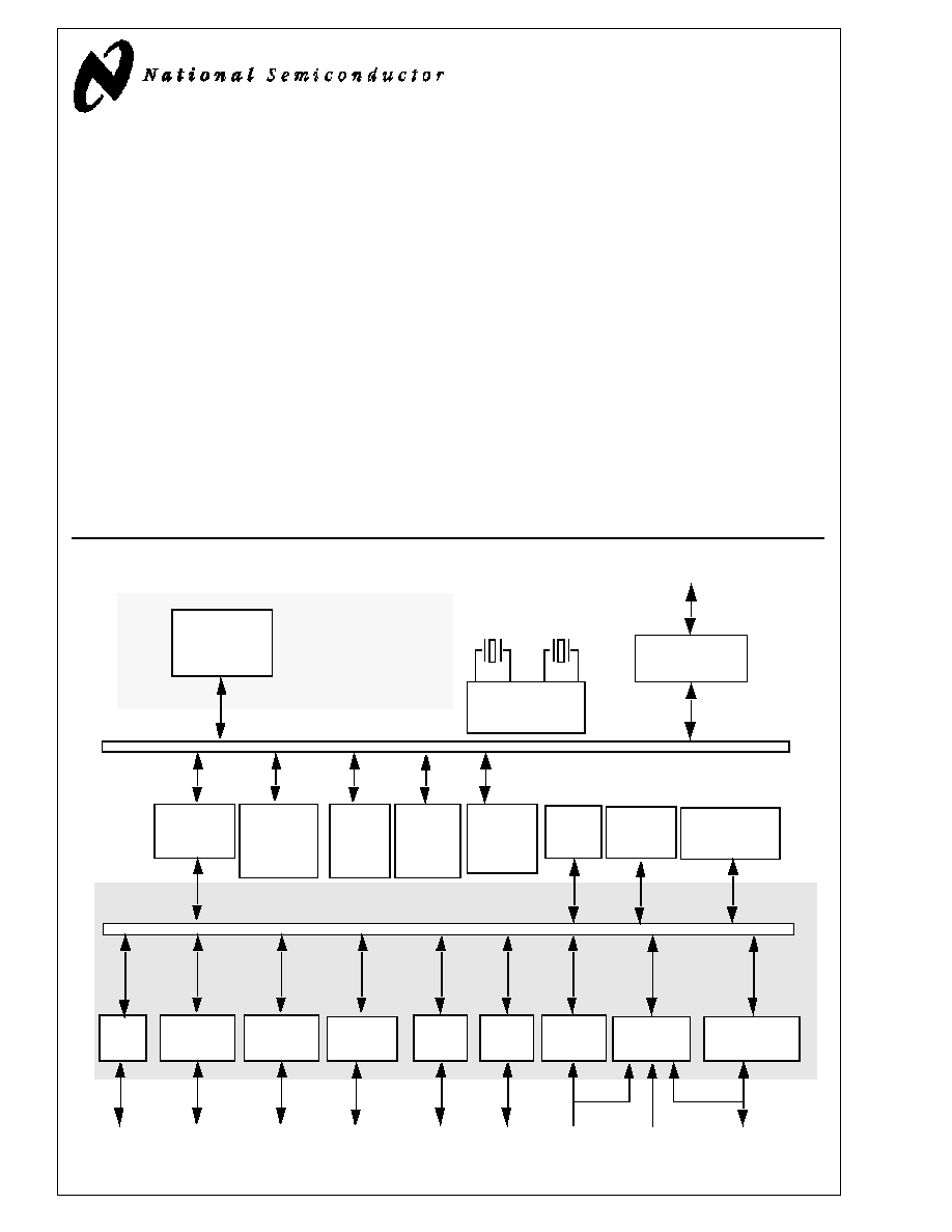
64k-Byte
Flash
Program
Memory
CR16CAN
Core Bus
Peripheral Bus
Clock Generator
Slow Clk*
Processing
Unit
I/O
µ
Wire/SPI
12-ch
Fast Clk
3k-Byte
Peripheral
Bus
Controller
Power-on-Reset
2176-Byte
RAM
EEPROM
Data
MIWU
2 Analog
Comparators
Timing and
Watchdog
Power
Manage-
ment
2x
MFT
2x
USART
CR16B
RISC Core
8-bit A/D
ACCESS
bus
4x
VTU
Memory
Memory
FullCAN 2.0B
1.5k-Byte
ISP
Please note that not all family members contain same peripheral modules and features.
Block Diagram

www.national.com
2
Table of Contents
1.0
General Description. . . . . . . . . . . . . . . . . . . . . . . . . . . . . . 1
2.0
Features . . . . . . . . . . . . . . . . . . . . . . . . . . . . . . . . . . . . . . . 3
3.0
Device Overview . . . . . . . . . . . . . . . . . . . . . . . . . . . . . . . . 5
3.1
CR16B CPU Core . . . . . . . . . . . . . . . . . . . . . . . . . . 5
3.2
Memory . . . . . . . . . . . . . . . . . . . . . . . . . . . . . . . . . .5
3.3
Input/Output Ports . . . . . . . . . . . . . . . . . . . . . . . . . . 5
3.4
Bus Interface Unit . . . . . . . . . . . . . . . . . . . . . . . . . . 5
3.5
Interrupts . . . . . . . . . . . . . . . . . . . . . . . . . . . . . . . . .5
3.6
Multi-Input Wake-up. . . . . . . . . . . . . . . . . . . . . . . . . 6
3.7
Dual Clock and Reset . . . . . . . . . . . . . . . . . . . . . . . 6
3.8
Power Management . . . . . . . . . . . . . . . . . . . . . . . . . 6
3.9
Multi-Function Timer . . . . . . . . . . . . . . . . . . . . . . . . 6
3.10 Versatile timer unit . . . . . . . . . . . . . . . . . . . . . . . . . . 6
3.11 Real-Time TIMER and Watchdog . . . . . . . . . . . . . . 6
3.12 USART . . . . . . . . . . . . . . . . . . . . . . . . . . . . . . . . . . .6
3.13 MICROWIRE/SPI . . . . . . . . . . . . . . . . . . . . . . . . . . . 6
3.14 CR16CAN . . . . . . . . . . . . . . . . . . . . . . . . . . . . . . . .7
3.15 ACCESS.bus Interface . . . . . . . . . . . . . . . . . . . . . . 7
3.16 A/D Converter . . . . . . . . . . . . . . . . . . . . . . . . . . . . . 7
3.17 Analog Comparators . . . . . . . . . . . . . . . . . . . . . . . . 7
3.18 Development Support . . . . . . . . . . . . . . . . . . . . . . . 7
4.0
Device Pinouts . . . . . . . . . . . . . . . . . . . . . . . . . . . . . . . . . . 8
4.1
Pin Description . . . . . . . . . . . . . . . . . . . . . . . . . . . . 10
5.0
System Configuration . . . . . . . . . . . . . . . . . . . . . . . . . . . 12
5.1
ENV0 and ENV1 Pins . . . . . . . . . . . . . . . . . . . . . . 12
5.2
Module Configuration (MCFG) Register . . . . . . . . 12
5.3
Module Status (MSTAT) Register . . . . . . . . . . . . . 12
6.0
Input/Output Ports . . . . . . . . . . . . . . . . . . . . . . . . . . . . . . 13
6.1
Port Registers . . . . . . . . . . . . . . . . . . . . . . . . . . . . 13
6.2
Open-Drain Operation . . . . . . . . . . . . . . . . . . . . . . 14
7.0
CPU and Core Registers . . . . . . . . . . . . . . . . . . . . . . . . . 15
7.1
General-Purpose Registers . . . . . . . . . . . . . . . . . .15
7.2
Dedicated Address Registers . . . . . . . . . . . . . . . . 15
7.3
Processor Status Register . . . . . . . . . . . . . . . . . . .15
7.4
Configuration Register . . . . . . . . . . . . . . . . . . . . . . 16
7.5
Addressing Modes . . . . . . . . . . . . . . . . . . . . . . . . . 16
7.6
Stacks . . . . . . . . . . . . . . . . . . . . . . . . . . . . . . . . . . 16
7.7
Instruction Set . . . . . . . . . . . . . . . . . . . . . . . . . . . . 16
8.0
Bus Interface Unit . . . . . . . . . . . . . . . . . . . . . . . . . . . . . . 18
8.1
Bus Cycles . . . . . . . . . . . . . . . . . . . . . . . . . . . . . . .18
8.2
BIU Control Registers . . . . . . . . . . . . . . . . . . . . . . 18
8.3
Wait and Hold States Used . . . . . . . . . . . . . . . . . .20
9.0
Memory . . . . . . . . . . . . . . . . . . . . . . . . . . . . . . . . . . . . . . . 22
9.1
Flash EEPROM Program Memory. . . . . . . . . . . . . 22
9.2
RAM Memory. . . . . . . . . . . . . . . . . . . . . . . . . . . . . 25
9.3
Flash EEPROM Data Memory. . . . . . . . . . . . . . . . 25
9.4
ISP Memory . . . . . . . . . . . . . . . . . . . . . . . . . . . . . . 27
10.0
Interrupts . . . . . . . . . . . . . . . . . . . . . . . . . . . . . . . . . . . . . 31
10.1 Interrupt Operation. . . . . . . . . . . . . . . . . . . . . . . . . 31
10.2 Non-Maskable Interrupt . . . . . . . . . . . . . . . . . . . . . 32
10.3 Maskable Interrupts . . . . . . . . . . . . . . . . . . . . . . . . 32
10.4 Interrupt Registers . . . . . . . . . . . . . . . . . . . . . . . . . 33
10.5 Interrupt Programming Procedures . . . . . . . . . . . . 35
11.0
Power Management . . . . . . . . . . . . . . . . . . . . . . . . . . . . . 36
11.1 Active Mode . . . . . . . . . . . . . . . . . . . . . . . . . . . . . . 36
11.2 Power Save Mode . . . . . . . . . . . . . . . . . . . . . . . . . 36
11.3 Idle Mode . . . . . . . . . . . . . . . . . . . . . . . . . . . . . . . .36
11.4 Halt Mode. . . . . . . . . . . . . . . . . . . . . . . . . . . . . . . .36
11.5 Clock Inputs and Reset Configuration . . . . . . . . . . 36
11.6 Switching Between Power Modes . . . . . . . . . . . . . 36
12.0
Dual Clock and Reset . . . . . . . . . . . . . . . . . . . . . . . . . . . 39
12.1 External Crystal Network . . . . . . . . . . . . . . . . . . . .39
12.2 Main System Clock . . . . . . . . . . . . . . . . . . . . . . . . 40
12.3 Slow System Clock . . . . . . . . . . . . . . . . . . . . . . . . 40
12.4 Power-On Reset . . . . . . . . . . . . . . . . . . . . . . . . . . 41
12.5 External Reset . . . . . . . . . . . . . . . . . . . . . . . . . . . . 41
12.6 Dual Clock and Reset Registers . . . . . . . . . . . . . . 41
12.7 Slow Clock Prescaler Register (PRSSC) . . . . . . . . 41
12.8 Slow Clock Prescaler 1 Register (PRSSC1) . . . . .41
13.0
Multi-Input Wake-Up . . . . . . . . . . . . . . . . . . . . . . . . . . . .42
13.1 Wake-Up Edge Detection Register (WKEDG) . . . .42
13.2 Wake-Up Enable Register (WKENA) . . . . . . . . . . .42
13.3 Wake-Up Interrupt Control Register 1 (WKCTRL1) 43
13.4 Wake-Up Interrupt Control Register 1 (WKCTRL2) 43
13.5 Wake-Up Pending Register (WKPND) . . . . . . . . . .43
13.6 Wake-Up Pending Clear Register (WKPCL) . . . . .43
13.7 Programming Procedures . . . . . . . . . . . . . . . . . . .44
14.0
Real-Time Timer and WATCHDOG . . . . . . . . . . . . . . . . .45
14.1 TWM Structure . . . . . . . . . . . . . . . . . . . . . . . . . . . .45
14.2 Timer T0 Operation . . . . . . . . . . . . . . . . . . . . . . . .45
14.3 WATCHDOG Operation . . . . . . . . . . . . . . . . . . . . .46
14.4 TWM Registers . . . . . . . . . . . . . . . . . . . . . . . . . . . .46
14.5 WATCHDOG Programming Procedure . . . . . . . . .47
15.0
Multi-Function Timer . . . . . . . . . . . . . . . . . . . . . . . . . . . .49
15.1 Timer Structure. . . . . . . . . . . . . . . . . . . . . . . . . . . .49
15.2 Timer Operating Modes . . . . . . . . . . . . . . . . . . . . .51
15.3 Timer Interrupts . . . . . . . . . . . . . . . . . . . . . . . . . . .54
15.4 Timer I/O Functions . . . . . . . . . . . . . . . . . . . . . . . .54
15.5 Timer Registers . . . . . . . . . . . . . . . . . . . . . . . . . . .56
16.0
Versatile-Timer-Unit (VTU) . . . . . . . . . . . . . . . . . . . . . . .58
16.1 VTU Functional Description . . . . . . . . . . . . . . . . . .58
16.2 VTU Registers . . . . . . . . . . . . . . . . . . . . . . . . . . . .61
17.0
MICROWIRE/SPI . . . . . . . . . . . . . . . . . . . . . . . . . . . . . . . .65
17.1 MICROWIRE Operation . . . . . . . . . . . . . . . . . . . . .65
17.2 Master Mode . . . . . . . . . . . . . . . . . . . . . . . . . . . . .66
17.3 Slave Mode . . . . . . . . . . . . . . . . . . . . . . . . . . . . . .67
17.4 Interrupt Generation . . . . . . . . . . . . . . . . . . . . . . . .68
17.5 MICROWIRE Interface Registers. . . . . . . . . . . . . .68
18.0
USART . . . . . . . . . . . . . . . . . . . . . . . . . . . . . . . . . . . . . . . .71
18.1 Functional Overview . . . . . . . . . . . . . . . . . . . . . . . .71
18.2 USART Operation . . . . . . . . . . . . . . . . . . . . . . . . .71
18.3 USART Registers . . . . . . . . . . . . . . . . . . . . . . . . . .75
18.4 Baud Rate Calculations . . . . . . . . . . . . . . . . . . . . .77
19.0
ACCESS.bus Interface . . . . . . . . . . . . . . . . . . . . . . . . . . .78
19.1 ACB Protocol Overview . . . . . . . . . . . . . . . . . . . . .78
19.2 ACB Functional Description . . . . . . . . . . . . . . . . . .79
19.3 ACB Registers . . . . . . . . . . . . . . . . . . . . . . . . . . . .82
19.4 Usage Hints . . . . . . . . . . . . . . . . . . . . . . . . . . . . . .84
20.0
CR16CAN Module. . . . . . . . . . . . . . . . . . . . . . . . . . . . . . .85
20.1 Functional Description . . . . . . . . . . . . . . . . . . . . . .85
20.2 Basic CAN Concepts . . . . . . . . . . . . . . . . . . . . . . .87
20.3 Message Transfer . . . . . . . . . . . . . . . . . . . . . . . . .95
20.4 Acceptance Filtering . . . . . . . . . . . . . . . . . . . . . . . .96
20.5 Receive Structure . . . . . . . . . . . . . . . . . . . . . . . . . .97
20.6 Transmit Structure . . . . . . . . . . . . . . . . . . . . . . . .100
20.7 Interrupts . . . . . . . . . . . . . . . . . . . . . . . . . . . . . . .103
20.8 Time Stamp Counter . . . . . . . . . . . . . . . . . . . . . .105
20.9 Memory Organization . . . . . . . . . . . . . . . . . . . . . .105
20.10 System Start-Up and Multi-Input Wake-Up . . . . .116
21.0
Analog Comparators . . . . . . . . . . . . . . . . . . . . . . . . . . . 118
21.1 Analog Comparator Control/Status Register
(CMPCTRL). . . . . . . . . . . . . . . . . . . . . . . . . . . . . .118
21.2 Analog Comparator Usage . . . . . . . . . . . . . . . . . .118
22.0
A/D Converter . . . . . . . . . . . . . . . . . . . . . . . . . . . . . . . . .119
22.1 Operating Modes . . . . . . . . . . . . . . . . . . . . . . . . .119
22.2 A/D Converter Registers . . . . . . . . . . . . . . . . . . .120
22.3 A/D Converter Programming . . . . . . . . . . . . . . . .122
23.0
Memory Map . . . . . . . . . . . . . . . . . . . . . . . . . . . . . . . . . .123
24.0
Register Layouts . . . . . . . . . . . . . . . . . . . . . . . . . . . . . . 129
24.1 Register layout . . . . . . . . . . . . . . . . . . . . . . . . . . .129
25.0
ELECTRICAL AND THERMAL CHARACTERISTICS . . 136
26.0
Appendix . . . . . . . . . . . . . . . . . . . . . . . . . . . . . . . . . . . . . 152
26.1 CR16CAN. . . . . . . . . . . . . . . . . . . . . . . . . . . . . . .152
26.2 8/16-bit microwire/spi (MWSPI16) . . . . . . . . . . . .154
26.3 Timing and watchdog module . . . . . . . . . . . . . . .154

3
www.national.com
1.0
General Description
(Continued)
The device has up to 64K bytes of reprogrammable flash EE-
PROM program memory or ROM memory, 1.5K bytes of
flash EEPROM In-System-Programming memory, 3K bytes
of static RAM, 2K bytes of non-volatile EEPROM data mem-
ory and 128 bytes with high endurance, two USARTs, two 16-
bit multi-function timers, one SPI/MICROWIRE-PLUSTM seri-
al interface, a 12-channel A/D converter, two analog compar-
ators, WATCHDOGTM protection mechanism, and up to 56
general-purpose I/O pins.
The device operates with a high-frequency crystal as the
main clock source and either the prescaled main clock
source or with a low frequency (32.768 kHz) oscillator in
Power Save mode. The device supports several Power Save
modes which are combined with multi-source interrupt and
wake-up capabilities.
This device also has a Versatile Timer Unit (VTU) with four
timer sub-systems, a CAN interface, and ACCESS.bus syn-
chronous serial bus interface.
Powerful cross-development tools are available from Nation-
al Semiconductor and third party suppliers to support the de-
velopment and debugging of application software for the
device. These tools let you program the application software
in C and are designed to take full advantage of the Compac-
tRISC architecture.
In the following text, device is always referred to the family of
16-bit CAN-enabled CompactRISC Microtroller.
2.0
Features
∑
CPU Features
-- Fully static core, capable of operating at any rate from
0 to 24 MHz (4 MHz minimum in active mode)
-- 50 ns instruction cycle time with a 20 MHz external
clock frequency
-- Multi-source vectored interrupts (internal, external,
and on-chip peripheral)
-- Dual clock and reset
∑
On-chip power-on reset
∑
On-Chip Memory
-- Up to 64K bytes flash EEPROM program memory; can
be programmed, erased, and reprogrammed by soft-
ware (100K cycles)
-- 3K bytes of static RAM data memory
-- For flash program memory devices, 1.5k bytes flash
EEPROM memory is available to store boot loader
code (100K cycles)
-- 2K bytes of non-volatile EEPROM data memory with
low endurance (25K cycles) and 128 bytes with high
endurance (100K cycles)
∑
On-Chip Peripherals
-- Two Universal Synchronous/Asynchronous Receiver/
Transmitter (USART) devices
-- Programmable Idle Timer and real-time clock (T0)
-- Two dual 16-bit multi-function timers (MFT1 and MFT2)
-- 8/16-bit SPI/MICROWIRE-PLUS serial interface
-- 12-channel, 8-bit Analog-to-Digital (A/D) converter
with external voltage reference, programmable sam-
ple-and-hold delay, and programmable conversion fre-
quency
-- ACCESS.bus synchronous serial bus
-- FullCAN interface with 15 message buffers complaint
to CAN specification 2.0B active
-- Versatile Timer Unit with four subsystems (VTU)
-- Two analog comparators
-- Integrated WATCHDOG logic
∑
I/O Features
-- Up to 56 general-purpose I/O pins (shared with on-chip
peripheral I/O pins)
-- Programmable I/O pin characteristics: TRI-STATE out-
put, push-pull output, weak pull-up input, high-imped-
ance input
-- Schmitt triggers on general purpose inputs
∑
Power Supply
-- 4.5V to 5.5V single-supply operation
∑
Temperature Range
-- ≠40
∞
C to +85
∞
C
-- ≠40
∞
C to +125
∞
C
∑
Development Support
-- Real-time emulation and full program debug capabili-
ties available
-- CompactRISC tools provide C programming and de-
bugging support
www.national.com
4
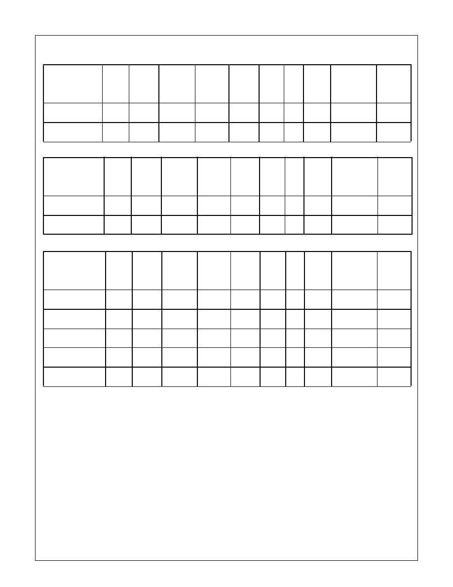
CR16 CompactRISC Microcontroller with CAN Interface Family Selection Guide
Programmable devices
Factory Programmed devices
ROM devices
Note:
All devices contains Access.bus (ACB), Clock and Re-
set, MICROWIRE/API, Multi-Input Wake-Up (MIWU), Power
Management (PMM), and the Real-Time Timer and Watch-
dog (TWM) modules. Access.bus is compatible with I2C bus
offered by Philips Semiconductor.
CR16 CompactRISC Microcontroller with CAN Interface
Family Devices
National Semiconductor currently offers a variety of the
CR16 CompactRISC Microcontrollers with CAN interface.
The CR16MCS offer complete functionality in an 80-pin
PQFP package.
NSID
Speed
(MHz)
Flash/
(kByte)
EEPROM
Data
Memory
(Bytes)
SRAM
(kBytes)
USART Timer I/Os
Temp.
Range
Peripherals
Package
Type
CR16MCS9VJEx
16
64
2176
3
2
2MFT,
VTU
56
E, I
ADC, CAN,
Comparators 80 PQFP
CR16MAS9VJEx
24
64
3
2
2MFT,
VTU
56
E, I
ADC, CAN,
Comparators 80 PQFP
NSID
Speed
(MHz)
Flash/
(KByte)
EEPROM
Data
Memory
(Bytes)
SRAM
(kBytes)
USART Timer
I/Os
Temp.
Range
Peripherals
Package
Type
CR16MCS9VJExy
16
64
2176
3
2
2MFT,
VTU
56
E, I
ADC, CAN,
Comparators 80 PQFP
CR16MCS9VJExy
24
64
2176
3
2
2MFT,
VTU
56
E, I
ADC, CAN,
Comparators
80 PQFP
NSID
Speed
(MHz)
Flash/
ROM
(KByte)
EEPROM
Data
Memory
(Bytes)
SRAM
(kBytes)
USART Timer I/Os
Temp.
Range
Peripherals
Package
Type
CR16HCS9VJEx
24
64
2176
3
2
2MFT,
VTU
56
E, I
ADC, CAN,
Comparators 80 PQFP
CR16MCS5VJEx
24
64
2176
3
2
2MFT,
VTU
56
E, I
ADC, CAN,
Comparators 80 PQFP
CR16MBR5VJEx
24
32
2176
3
2
2MFT,
VTU
56
E, I
ADC, CAN,
Comparators
80 PQFP
CR16MAR5VJEx
24
32
3
2
2MFT,
VTU
56
E, I
CAN,
80 PQFP
CR16MAS5VJEx
24
64
3
2
2MFT,
VTU
56
E, I
CAN,
80 PQFP
Note:
∑
Suffix x in the NSID is defined below:
Temperature Ranges:
I = Industrial
E = Extended
∑
Suffix y in the NSID defines the ROM code.
-40
∞
C to +85
∞
C is represented when x is 8
-40
∞
C to +125
∞
C is represented when x is 7

5
www.national.com
3.0
Device Overview
The devices are complete microcomputers with all system
timing, interrupt logic, program memory, data memory, and I/
O ports included on-chip, making it well-suited to a wide
range of embedded controller applications.
3.1
CR16B CPU CORE
The device uses a CR16B CPU core module. This is the
same core used in other CompactRISC family member de-
signs, like DECT or GSM chipsets.
The high performance of the CPU core results from the im-
plementation of a pipelined architecture with a two-bytes-per-
cycle pipelined system bus. As a result, the CPU can support
a peak execution rate of one instruction per clock cycle.
Compared with conventional RISC processors, the device
differs in the following ways:
-- The CPU core can use on-chip rather than external
memory. This eliminates the need for large and com-
plex bus interface units.
-- Most instructions are 16 bits, so all basic instructions
are just two bytes long. Additional bytes are sometimes
required for immediate values, so instructions can be
two or four bytes long.
-- Non-aligned word access is allowed. Each instruction
can operate on 8-bit or 16-bit data.
-- The device is designed to operate with a clock rate in
the 10 to 24 MHz range rather than 100 MHz or more.
Most embedded systems face EMI and noise con-
straints that limit clock speed to these lower ranges. A
lower clock speed means a simpler, less costly silicon
implementation.
-- The instruction pipeline uses three stages. A smaller
pipeline eliminates the need for costly branch predic-
tion mechanisms and bypass registers, while maintain-
ing adequate performance for typical embedded
controller applications.
For more information, please refer to the CR16B Program-
mer's Reference Manual, Literature #: 633150.
3.2
MEMORY
The CompactRISC architecture supports a uniform linear ad-
dress space of 2 megabytes. The device implementation of
this architecture uses only the lowest 128K bytes of address
space. Four types of on-chip memory occupy specific inter-
vals within this address space:
∑
64K bytes of flash EEPROM program memory (100K cy-
cles)
∑
48K bytes ROM programm memory version available also
(100K cycles)
∑
3K bytes of static RAM
∑
2K bytes of EEPROM data memory with low endurance
(25K cycles)
∑
128 bytes with high endurance (100K cycles)
∑
1.5K bytes flash EEPROM memory for ISP code
The 3K bytes of static RAM are used for temporary storage
of data and for the program stack and interrupt stack. Read
and write operations can be byte-wide or word-wide, depend-
ing on the instruction executed by the CPU. Each memory
access requires one clock cycle; no wait cycles or hold cycles
are required.
There are two types of flash EEPROM data memory storage.
The 2K bytes of EEPROM data memory with low endurance
(25K cycles) and 128 bytes of flash EEPROM data memory
with high endurance (100K cycles) are used for non-volatile
storage of data, such as configuration settings entered by the
end-user.
The 64K bytes of flash EEPROM program memory are used
to store the application program. It has security features to
prevent unintentional programming and to prevent unautho-
rized access to the program code. This memory can be pro-
grammed with a device external programming unit or with the
device installed in the application system (in-system pro-
gramming).
There is a factory programmed boot memory used to store
In-System-Programming (ISP) code. (This code allows pro-
gramming of the program memory via one of the USART in-
terfaces in the final application.)
For flash EEPROM program and data memory, the device in-
ternally generates the necessary voltages for programming.
No additional power supply is required.
3.3
INPUT/OUTPUT PORTS
The device has 56 software-configurable I/O pins, organized
into seven 8-pin ports called Port B, Port C, Port F, Port G,
Port H, Port I, and Port L. Each pin can be configured to op-
erate as a general-purpose input or general-purpose output.
In addition, many I/O pins can be configured to operate as a
designated input or output for an on-chip peripheral module
such as the USART, timer, A/D converter, or MICROWIRE/
SPI interface.
The I/O pin characteristics are fully programmable. Each pin
can be configured to operate as a TRI-STATE output, push-
pull output, weak pull-up input, or high-impedance input.
3.4
BUS INTERFACE UNIT
The Bus Interface Unit (BIU) controls the interface between
the on-chip modules to the internal core bus. It determines
the configured parameters for bus access (such as the num-
ber of wait states for memory access) and issues the appro-
priate bus signals for each requested access.
The BIU uses a set of control registers to determine how
many wait states and hold states are to be used when ac-
cessing flash EEPROM program memory, ISP memory and
the I/O area (Port B and Port C). Upon start-up the configu-
ration registers are set for slowest possible memory access.
To achieve fastest possible program execution, appropriate
values should be programmed. These settings vary with the
clock frequency and the type of on-chip device being access-
ed.