©2001 National Semiconductor Corporation
www.national.com
C
R
1
6
M
E
S
5
/
C
R
1
6
M
E
S
9
/
C
R
1
6
M
F
S
5
/
C
R
1
6
M
F
S
9
/
C
R
1
6
M
H
S
5
/
C
R
1
6
M
H
S
9
/
C
R
1
6
M
N
S
5
/
C
R
1
6
M
N
S
9
/
C
R
1
6
M
9
S
5
/
C
R
1
6
M
U
S
5
/
C
R
1
6
M
U
S
9
/
F
a
m
i
l
y
o
f
C
o
m
p
a
c
t
R
I
S
C
1
6
-
B
i
t
M
i
c
r
o
c
o
n
t
r
o
l
l
e
r
s
December 2001
CR16MES5/CR16MES9/CR16MFS5/CR16MFS9/
CR16MHS5/CR16MHS9/CR16MNS5/CR16MNS9/
CR16M9S5/CR16MUS5/CR16MUS9/
Family of CompactRISC 16-Bit Microcontrollers
1.0
General Description
The family of CompactRISCTM microcontrollers are gener-
al-purpose 16-bit microcontrollers based on a Reduced In-
struction Set Computer (RISC) architecture. The device
operates as a complete microcomputer with all system tim-
ing, interrupt logic, flash program memory or ROM memo-
ry, RAM, EEPROM data memory, and I/O ports included
on-chip. It is ideally suited to a wide range of embedded
controller applications because of its high performance,
on-chip integrated features and low power consumption,
resulting in decreased system cost.
The family of CompactRISC 16-bit microcontrollers offer
the high performance of a RISC architecture while retain-
ing the advantages of a traditional Complex Instruction Set
Computer (CISC): compact code, on-chip memory and I/O,
and reduced cost. The CPU uses a three-stage instruction
pipeline that allows execution of up to one instruction per
clock cycle, or up to 20 million instructions per second (MI-
PS) at a clock rate of 20 MHz.
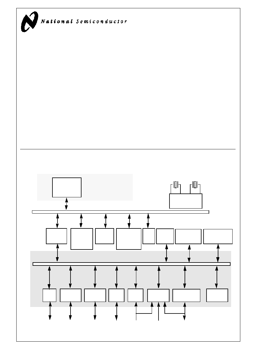
CR16B
Core
Core Bus
Peripheral Bus
Clock Generator
Slow Osc
Processing
Unit
I/O
µ
Wire/SPI
A/D
Fast Osc
2 kbyte
Interrupt
Control
(ICU)
Peripheral
Bus
Controller
Power-on-Reset
RAM
48k Flash
Program
Memory
Two Analog
Comparators
Real-Time
Timer
WATCHDOG
Power-Save
Management
Two
MFTs
Two
USARTs
TRI-STATEÆ is a registered trademark of National Semiconductor Corporation.
640 Bytes
EEPROM
Data
Memory
boot
MIWU
ROM
Please note that not all family members contain same peripheral modules and features.
Block Diagram

www.national.com
2
Table of Contents
1.0
General Description. . . . . . . . . . . . . . . . . . . . . . . . . . . . . . 1
2.0
Features . . . . . . . . . . . . . . . . . . . . . . . . . . . . . . . . . . . . . . . 3
3.0
Device Overview . . . . . . . . . . . . . . . . . . . . . . . . . . . . . . . . 5
3.1
CR16B CPU Core . . . . . . . . . . . . . . . . . . . . . . . . . . 5
3.2
Memory . . . . . . . . . . . . . . . . . . . . . . . . . . . . . . . . . .5
3.3
Input/Output Ports . . . . . . . . . . . . . . . . . . . . . . . . . . 5
3.4
Bus Interface Unit . . . . . . . . . . . . . . . . . . . . . . . . . . 5
3.5
Interrupts . . . . . . . . . . . . . . . . . . . . . . . . . . . . . . . . .5
3.6
Multi-Input Wake-up. . . . . . . . . . . . . . . . . . . . . . . . . 6
3.7
Dual Clock and Reset . . . . . . . . . . . . . . . . . . . . . . . 6
3.8
Power Management . . . . . . . . . . . . . . . . . . . . . . . . . 6
3.9
Multi-Function Timer . . . . . . . . . . . . . . . . . . . . . . . . 6
3.10 Real-Time TIMER and Watchdog . . . . . . . . . . . . . . 6
3.11 USART . . . . . . . . . . . . . . . . . . . . . . . . . . . . . . . . . . .6
3.12 MICROWIRE/SPI . . . . . . . . . . . . . . . . . . . . . . . . . . . 6
3.13 A/D Converter . . . . . . . . . . . . . . . . . . . . . . . . . . . . . 6
3.14 Analog Comparators . . . . . . . . . . . . . . . . . . . . . . . . 7
3.15 Development Support . . . . . . . . . . . . . . . . . . . . . . . 7
3.16 Pin Description . . . . . . . . . . . . . . . . . . . . . . . . . . . . 10
4.0
System Configuration . . . . . . . . . . . . . . . . . . . . . . . . . . . 12
4.1
ENV0 and ENV1 Pins . . . . . . . . . . . . . . . . . . . . . . 12
4.2
Module Configuration (MCFG) Register . . . . . . . . 12
4.3
Module Status (MSTAT) Register . . . . . . . . . . . . . 12
5.0
Input/Output Ports . . . . . . . . . . . . . . . . . . . . . . . . . . . . . . 13
5.1
Port Registers . . . . . . . . . . . . . . . . . . . . . . . . . . . . 13
5.2
Open-Drain Operation . . . . . . . . . . . . . . . . . . . . . . 14
6.0
CPU and Core Registers . . . . . . . . . . . . . . . . . . . . . . . . . 15
6.1
General-Purpose Registers . . . . . . . . . . . . . . . . . .15
6.2
Dedicated Address Registers . . . . . . . . . . . . . . . . 15
6.3
Processor Status Register . . . . . . . . . . . . . . . . . . .15
6.4
Configuration Register . . . . . . . . . . . . . . . . . . . . . . 16
6.5
Addressing Modes . . . . . . . . . . . . . . . . . . . . . . . . . 16
6.6
Stacks . . . . . . . . . . . . . . . . . . . . . . . . . . . . . . . . . . 16
6.7
Instruction Set . . . . . . . . . . . . . . . . . . . . . . . . . . . . 16
7.0
Bus Interface Unit . . . . . . . . . . . . . . . . . . . . . . . . . . . . . . 18
7.1
Bus Cycles . . . . . . . . . . . . . . . . . . . . . . . . . . . . . . .18
7.2
BIU Control Registers . . . . . . . . . . . . . . . . . . . . . . 18
7.3
Wait and Hold States Used . . . . . . . . . . . . . . . . . .19
8.0
Memory . . . . . . . . . . . . . . . . . . . . . . . . . . . . . . . . . . . . . . . 21
8.1
Flash Program Memory . . . . . . . . . . . . . . . . . . . . . 21
8.2
RAM Memory. . . . . . . . . . . . . . . . . . . . . . . . . . . . . 24
8.3
EEPROM Data Memory. . . . . . . . . . . . . . . . . . . . . 24
8.4
ISP Memory . . . . . . . . . . . . . . . . . . . . . . . . . . . . . . 24
9.0
Interrupts . . . . . . . . . . . . . . . . . . . . . . . . . . . . . . . . . . . . . 27
9.1
Interrupt Operation. . . . . . . . . . . . . . . . . . . . . . . . . 27
9.2
Non-Maskable Interrupt . . . . . . . . . . . . . . . . . . . . . 28
9.3
Maskable Interrupts . . . . . . . . . . . . . . . . . . . . . . . . 29
9.4
Interrupt Registers . . . . . . . . . . . . . . . . . . . . . . . . . 29
9.5
Interrupt Programming Procedures . . . . . . . . . . . . 31
10.0
Power Management . . . . . . . . . . . . . . . . . . . . . . . . . . . . . 33
10.1 Active Mode . . . . . . . . . . . . . . . . . . . . . . . . . . . . . . 33
10.2 Power Save Mode . . . . . . . . . . . . . . . . . . . . . . . . . 33
10.3 Idle Mode . . . . . . . . . . . . . . . . . . . . . . . . . . . . . . . .33
10.4 Halt Mode. . . . . . . . . . . . . . . . . . . . . . . . . . . . . . . .33
10.5 Switching Between Power Modes . . . . . . . . . . . . . 33
11.0
Dual Clock and Reset . . . . . . . . . . . . . . . . . . . . . . . . . . .36
11.1 External Crystal Network . . . . . . . . . . . . . . . . . . . .36
11.2 Main System Clock . . . . . . . . . . . . . . . . . . . . . . . . .37
11.3 Slow System Clock . . . . . . . . . . . . . . . . . . . . . . . . .37
11.4 Power-On Reset . . . . . . . . . . . . . . . . . . . . . . . . . . .38
11.5 External Reset . . . . . . . . . . . . . . . . . . . . . . . . . . . .38
11.6 Dual Clock and Reset Registers . . . . . . . . . . . . . .38
11.7 Slow Clock Prescaler Register (PRSSC) . . . . . . . .38
12.0
Multi-Input Wake-Up . . . . . . . . . . . . . . . . . . . . . . . . . . . .39
12.1 Wake-Up Edge Detection Register (WKEDG) . . . .39
12.2 Wake-Up Enable Register (WKENA) . . . . . . . . . . .39
12.3 Wake-Up Source Select Register (WKCTRL) . . . .40
12.4 Wake-Up Pending Register (WKPND) . . . . . . . . . .40
12.5 Wake-Up Pending Clear Register (WKPCL) . . . . .40
12.6 Programming Procedures . . . . . . . . . . . . . . . . . . .40
13.0
Real-Time Timer and WATCHDOG . . . . . . . . . . . . . . . . .41
13.1 TWM Structure . . . . . . . . . . . . . . . . . . . . . . . . . . . .41
13.2 Timer T0 Operation . . . . . . . . . . . . . . . . . . . . . . . .41
13.3 WATCHDOG Operation . . . . . . . . . . . . . . . . . . . . .42
13.4 TWM Registers . . . . . . . . . . . . . . . . . . . . . . . . . . . .42
13.5 WATCHDOG Programming Procedure . . . . . . . . .43
14.0
Multi-Function Timer . . . . . . . . . . . . . . . . . . . . . . . . . . . .45
14.1 Timer Structure. . . . . . . . . . . . . . . . . . . . . . . . . . . .45
14.2 Timer Operating Modes . . . . . . . . . . . . . . . . . . . . .47
14.3 Timer Interrupts . . . . . . . . . . . . . . . . . . . . . . . . . . .50
14.4 Timer I/O Functions . . . . . . . . . . . . . . . . . . . . . . . .50
14.5 Timer Registers . . . . . . . . . . . . . . . . . . . . . . . . . . .51
15.0
MICROWIRE/SPI . . . . . . . . . . . . . . . . . . . . . . . . . . . . . . . .54
15.1 MICROWIRE Operation . . . . . . . . . . . . . . . . . . . . .54
15.2 Master Mode . . . . . . . . . . . . . . . . . . . . . . . . . . . . .55
15.3 Slave Mode . . . . . . . . . . . . . . . . . . . . . . . . . . . . . .56
15.4 Interrupt Generation . . . . . . . . . . . . . . . . . . . . . . . .57
15.5 MICROWIRE Interface Registers. . . . . . . . . . . . . .58
16.0
USART . . . . . . . . . . . . . . . . . . . . . . . . . . . . . . . . . . . . . . . .61
16.1 Functional Overview . . . . . . . . . . . . . . . . . . . . . . . .61
16.2 USART Operation . . . . . . . . . . . . . . . . . . . . . . . . .61
16.3 USART Registers . . . . . . . . . . . . . . . . . . . . . . . . . .65
16.4 Baud Rate Calculations . . . . . . . . . . . . . . . . . . . . .67
17.0
Analog Comparators . . . . . . . . . . . . . . . . . . . . . . . . . . . .68
17.1 Analog Comparator Control/Status Register
(CMPCTRL)68
17.2 Analog Comparator Usage . . . . . . . . . . . . . . . . . . .68
18.0
A/D Converter . . . . . . . . . . . . . . . . . . . . . . . . . . . . . . . . . .69
18.1 Operating Modes . . . . . . . . . . . . . . . . . . . . . . . . . .69
18.2 A/D Converter Registers . . . . . . . . . . . . . . . . . . . .70
18.3 A/D Converter Programming . . . . . . . . . . . . . . . . .72
19.0
Memory Map . . . . . . . . . . . . . . . . . . . . . . . . . . . . . . . . . . .73
20.0
Register Layouts . . . . . . . . . . . . . . . . . . . . . . . . . . . . . . .77
20.1 Register layout . . . . . . . . . . . . . . . . . . . . . . . . . . . .77
21.0
ELECTRICAL CHARACTERISTICS . . . . . . . . . . . . . . . . .81
Comparator AC and DC Characteristics . . . . . . . . . . . .83
Output Signal Levels . . . . . . . . . . . . . . . . . . . . . . . . . . . .85
22.0
Appendix . . . . . . . . . . . . . . . . . . . . . . . . . . . . . . . . . . . . . .95
22.1 8-bit MICROWIRE/SPI (MWSPI) . . . . . . . . . . . . . .95
22.2 Timing and watchdog module . . . . . . . . . . . . . . . .95
23.0
Physical Dimension . . . . . . . . . . . . . . . . . . . . . . . . . . . . .97

3
www.national.com
1.0
General Description
(Continued)
In the following text, device is alsays refered to the family of
CompactRISC 16-bit microcontrollers. For the exact feature
set, check individual datasheets.
The device is available in a variety of package sizes and
types. All devices have 48 kbytes of reprogrammable flash
program memory, 1.5 kbytes of ISP memory, 2 kbytes of stat-
ic RAM, and 640 bytes of non-volatile EEPROM data memo-
ry. The 80-pin device has two USARTs, two 16-bit multi-
function timers, one SPI/MICROWIRE-PLUSTM serial inter-
face, an 8-channel A/D converter, two analog comparators,
WATCHDOGTM protection mechanism, and up to 48 general-
purpose I/O pins. The 44-pin devices offer the same basic
features as the 80-pin device, but with fewer I/O ports and
peripheral modules due to the smaller number of available
pins.
All devices operate with a high-frequency crystal as the main
clock source. Some packages allow the device to operate
with either the main clock source or with a slow (32.768 KHz)
oscillator in Power Save mode. The device supports several
Power Save modes which are combined with multi-source in-
terrupt and wake-up capabilities.
Powerful cross-development tools are available from Nation-
al Semiconductor and third party suppliers to support the de-
velopment and debugging of application software for the
device. These tools let you program the application software
in C and are designed to take full advantage of the Compac-
tRISC architecture.
2.0
Features
∑
CPU Features
-- Fully static core, capable of operating at any rate from
0 to 20 MHz (4 MHz minimum in active mode)
-- 50 ns instruction cycle time with a 20 MHz external
clock frequency
-- Multi-source vectored interrupts (internal, external,
and on-chip peripheral)
-- On-chip power-on reset
∑
On-Chip Memory
-- 48 kbytes of flash program memory or ROM memory
(100K cycle)
-- 1.5 kbytes of ISP memory (100K cycle)
-- 2 kbytes of static RAM data memory
-- 640 bytes of non-volatile EEPROM data memory,
word-programmable (100K cycle)
∑
On-Chip Peripherals
-- Up to two Universal Synchronous/Asynchronous Re-
ceiver/Transmitter (USART) devices
-- Programmable Idle Timer and real-time clock (T0)
-- Up to two dual 16-bit multi-function timers (MFT1 and
MFT2)
-- SPI/MICROWIRE-PLUS serial interface
-- 8-channel, 8-bit Analog-to-Digital (A/D) converter with
external voltage reference, programmable sample-
and-hold delay, and programmable conversion fre-
quency
-- Up to two analog comparators
-- Integrated WATCHDOG logic
∑
I/O Features
-- Up to 48 general-purpose I/O pins (shared with on-chip
peripheral I/O pins)
-- Programmable I/O pin characteristics: TRI-STATE out-
put, push-pull output, weak pull-up input, high-imped-
ance input
-- Software-configurable Schmitt triggers on inputs
∑
Power Supply
-- 4.5V to 5.5V single-supply operation
∑
Temperature Range
-- 0
∞
C to +70
∞
C
-- ≠40
∞
C to +85
∞
C
-- ≠40
∞
C to +125
∞
C
∑
Development Support
-- Real-time emulation and full program debug capabili-
ties available
-- CompactRISC tools provide C programming and de-
bugging support
www.national.com
4
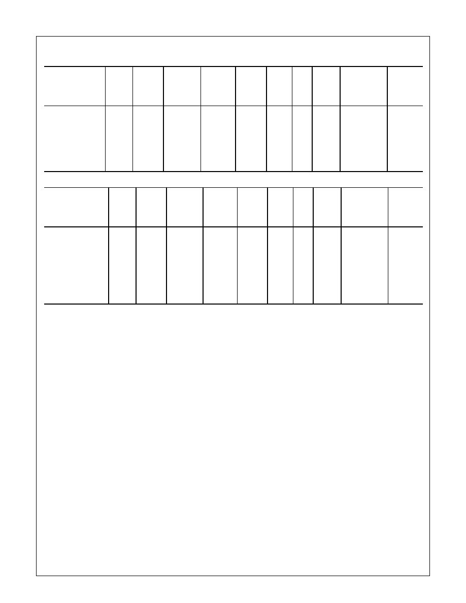
CR16 CompactRISC microcontroller Family Selection Guide
Programmable devices
ROM devices
Note:
All devices contains Clock and Reset, MICROWIRE/
API, Multi-Input Wake-Up (MIWU), Power Management
(PMM), and the Real-Time Timer and Watchdog (TWM) mod-
ules.
44-Pin PLCC versus 80-Pin PQFP
For 44PLCC packages, MICROWIRE/SPI slave mode, the
first 4 MIWU channels and the Vref pin are not available. 80-
pin PQFP packages provide the MICROWIRE/SPI master
and slave modes, 8 MIWU channels, Vref pin, and two US-
ARTs and two MFTs.
NSID
Speed
(MHz)
Flash/
ROM
(kByte)
EEPROM
Data
Memory
(Bytes)
SRAM
(kBytes)
USART Timer I/Os
Temp.
Range
Peripherals
Package
Type
CR16MHS9VJEx
20
48
640
2
2
2
48
E, I
ADC,
Comparators 80PQFP
CR16MFS944Vx
20
48
640
2
2
1
33
E, I
ADC
44PLCC
CR16MES944Vx
20
48
640
2
1
2
33
E, I
ADC
44PLCC
CR16MNS944Vx
20
48
None
2
1
2
33
C, I
None
44PLCC
CR16MUS944Vx
8
48
None
2
1
2
33
C
None
44PLCC
NSID
Speed
(MHz)
Flash/
ROM
(kByte)
EEPROM
Data
Memory
(Bytes)
SRAM
(kBytes)
USART Timer I/Os
Temp.
Range
Peripherals
Package
Type
CR16MHS5VJExy
20
48
640
2
2
2
48
E, I
ADC,
Comparators 80PQFP
CR16MFS544Vxy
20
48
640
2
2
1
33
E, I
ADC
44PLCC
CR16MES544Vxy
20
48
640
2
1
2
33
E, I
ADC
44PLCC
CR16MPS544Vxy
20
48
None
2
1
2
33
C, I
ADC
44PLCC
CR16MNS544Vxy
20
48
None
2
1
2
33
C, I
None
44PLCC
CR16MUS544Vxy
8
48
None
2
1
2
33
C
None
44PLCC
Note:
∑
Suffix x in the NSID is defined below:
Temperature Ranges:
E = Extended
I = Industrial
C = Commercial
∑
Suffix y in the NSID defines the ROM code.
-40
∞
C to +125
∞
C is represented when x is 7
-40
∞
C to +85
∞
C is represented when x is 8
0
∞
C to +70
∞
C is represented when x is 9

5
www.national.com
3.0
Device Overview
The family of CompactRISC 16-bit microcontrollers are com-
plete microcomputers with all system timing, interrupt logic,
program memory, data memory, and I/O ports included on-
chip, making it well-suited to a wide range of embedded con-
troller applications.
3.1
CR16B CPU CORE
The device uses the CR16B CPU core module. This is the
same core used in other CompactRISC family members.
The high performance of the CPU core results from the im-
plementation of a pipelined architecture with a two-bytes-per-
cycle pipelined system bus. As a result, the CPU can support
a peak execution rate of one instruction per clock cycle.
Compared with conventional RISC processors, the device
differs in the following ways:
∑
The CPU core uses on-chip rather than external memory.
This eliminates the need for large and complex bus inter-
face units.
∑
Most instructions are 16 bits, so all basic instructions are
just two bytes long. (Additional bytes are sometimes re-
quired for immediate values, so instructions can be two or
four bytes long.)
∑
Non-aligned word access is allowed. Each instruction can
operate on 8-bit or 16-bit.
∑
The device is designed to operate with a clock rate in the
10 to 25 MHz range rather than 100 MHz or more. Most
embedded systems face EMI and noise constraints that
limit clock speed to these lower ranges. A lower clock
speed means a simpler, less costly silicon implementa-
tion.
∑
The instruction pipeline uses three stages. A smaller pipe-
line eliminates the need for costly branch prediction
mechanisms and bypass registers, while maintaining ad-
equate performance for typical embedded controller ap-
plications.
3.2
MEMORY
The CompactRISC architecture supports a uniform linear ad-
dress space of 2 megabytes. The device implementation of
this architecture uses only the lowest 64 kbytes of address
space. Four types of on-chip memory occupy specific inter-
vals within this address space: 48 kbytes of flash program
memory, 1.5 kbytes of ISP memory, 2 kbytes of static RAM,
and 640 bytes of EEPROM data memory.
The 48 kbytes of flash program memory are used to store the
application program. It has security features to prevent unin-
tentional programming and to prevent unauthorized access
to the program code. This memory can be programmed ei-
ther with the device plugged into an EPROM programmer
unit (external programming) or with the device installed in the
application system (in-system programming).
The 2 kbytes of static RAM are used for temporary storage of
data and for the program stack and interrupt stack. Read and
write operations can be byte-wide or word-wide, depending
on the instruction executed by the CPU. Each memory ac-
cess requires one clock cycle; no wait cycles or hold cycles
are required.
The 640 bytes of EEPROM data memory are used for non-
volatile storage of data, such as configuration settings en-
tered by the end-user. The CPU reads or writes this memory
by using ordinary byte-wide or word-wide memory access
commands. After the CPU performs a write to this memory,
the on-chip hardware completes the EEPROM programming
in the background. A register status bit indicates the status of
the EEPROM programming operation.
There is a factory programmed boot memory used to store
In-System-Programming (ISP) code. (this code allows pro-
gramming of the program memory via one of the USART in-
terfaces in the final application.)
For the flash program memory, the device internally gener-
ates the necessary voltages for programming. No additional
power supply is required.
3.3
INPUT/OUTPUT PORTS
Each device has 48 software-configurable I/O pins, orga-
nized into six 8-pin ports called Port B, Port C, Port F, Port G,
Port L, and Port I. Each pin can be configured to operate as
a general-purpose input or general-purpose output. In addi-
tion, many I/O pins can be configured to operate as a desig-
nated input or output for an on-chip peripheral module such
as the USART, timer, A/D converter, or MICROWIRE/SPI in-
terface.
The I/O pin characteristics are fully programmable. Each pin
can be configured to operate as a TRI-STATE output, push-
pull output, weak pull-up input, or high-impedance input. In-
put pins can be software-configured to use Schmitt triggers
for noise resistance.
Each 44-pin device has a subset of the pins available in the
80-pin device. This results in the loss of some features that
are available in the larger-package device:
∑
One of the two USARTs or one of the two multi-function
timers (depending on package selection)
∑
Synchronous mode in the remaining USART(s)
∑
Slave mode operation for the MICROWIRE/SPI interface
∑
Separate external VREF for the A/D converter
∑
Comparators
∑
Four of the eight Multi-Input Wakeup pins
∑
NMI interrupt input pin
3.4
BUS INTERFACE UNIT
The Bus Interface Unit (BIU) controls the interface between
the on-chip modules to the internal core bus. It determines
the configured parameters for bus access (such as the num-
ber of wait states for memory access) and issues the appro-
priate bus signals for each requested access.
The BIU uses a set of control registers to determine how
many wait states and hold states are to be used when ac-
cessing EEPROM memory. Upon start-up of the device,
these registers must be programmed with appropriate values
so that the minimum allowable number states is used. This
number varies with the clock frequency and the type of on-
chip device being accessed.