DAC082S085
8-Bit Micro Power DUAL Digital-to-Analog Converter with
Rail-to-Rail Output
General Description
The DAC082S085 is a full-featured, general purpose DUAL
8-bit voltage-output digital-to-analog converter (DAC) that
can operate from a single +2.7V to 5.5V supply and con-
sumes 210 µA at 3V and 320 µA at 5V. The DAC082S085 is
packaged in 10-lead LLP and MSOP packages. The 10-lead
LLP package makes the DAC082S085 the smallest DUAL
DAC in its class. The on-chip output amplifier allows rail-to-
rail output swing and the three wire serial interface operates
at clock rates up to 40 MHz over the entire supply voltage
range. Competitive devices are limited to 25 MHz clock rates
at supply voltages in the 2.7V to 3.6V range. The serial
interface is compatible with standard SPI
TM
, QSPI, MI-
CROWIRE and DSP interfaces.
The reference for the DAC082S085 serves both channels
and can vary in voltage between 1V and V
A
, providing the
widest possible output dynamic range. The DAC082S085
has a 16-bit input shift register that controls the outputs to be
updated, the mode of operation, the powerdown condition,
and the binary input data. Both outputs can be updated
simultaneously or individually depending on the setting of
the two mode of operation bits.
A power-on reset circuit ensures that the DAC output powers
up to zero volts and remains there until there is a valid write
to the device. A power-down feature reduces power con-
sumption to less than a microWatt with three different termi-
nation options.
The low power consumption and small packages of the
DAC082S085 make it an excellent choice for use in battery
operated equipment.
The DAC082S085 is one of a family of pin compatible DACs,
including
the
10-bit
DAC102S085
and
the
12-bit
DAC124S085. The DAC082S085 operates over the ex-
tended industrial temperature range of -40∞C to +105∞C.
Features
n
Guaranteed Monotonicity
n
Low Power Operation
n
Rail-to-Rail Voltage Output
n
Power-on Reset to 0V
n
Simultaneous Output Updating
n
Wide power supply range (+2.7V to +5.5V)
n
Industry's Smallest Package
n
Power Down Modes
Key Specifications
n
Resolution
8 bits
n
INL
±
0.5 LSB (max)
n
DNL
+0.18 / -0.13 LSB (max)
n
Settling Time
4.5 µs (max)
n
Zero Code Error
+15 mV (max)
n
Full-Scale Error
-0.75 %FS (max)
n
Power Consumption
-- Normal
270 µA (3.6V) / 410 µA (5.5V) max
-- Pwr Down
20 nA (3.6V) / 30 nA (5.5V) typ
Applications
n
Battery-Powered Instruments
n
Digital Gain and Offset Adjustment
n
Programmable Voltage & Current Sources
n
Programmable Attenuators
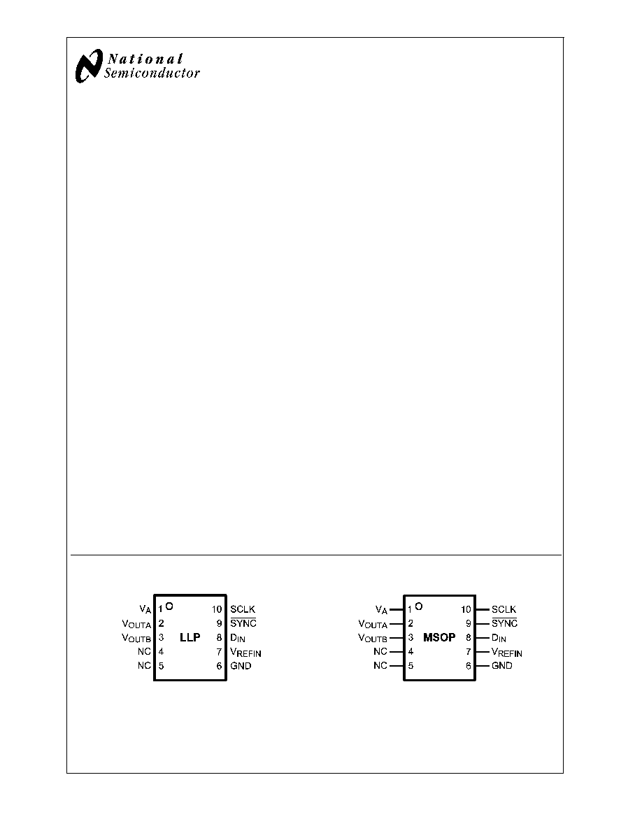
Pin Configuration
20195601
20195602
SPI
TM
is a trademark of Motorola, Inc.
PRELIMINARY
May 2006
DAC082S085
8-Bit
Micro
Power
DUAL
Digital-to-Analog
Converter
with
Rail-to-Rail
Output
© 2006 National Semiconductor Corporation
DS201956
www.national.com

Ordering Information
Order Numbers
Temperature Range
Package
Top Mark
DAC082S085CISD
-40∞C
T
A
+105∞C
LLP
X77C
DAC082S085CISDX
-40∞C
T
A
+105∞C
LLP Tape-and-Reel
X77C
DAC082S085CIMM
-40∞C
T
A
+105∞C
MSOP
X76C
DAC082S085CIMMX
-40∞C
T
A
+105∞C
MSOP Tape-and-Reel
X76C
DAC082S085EVAL
Evaluation Board
Block Diagram
20195603
DAC082S085
www.national.com
2
Pin Descriptions
LLP
MSOP
Pin No.
Symbol
Type
Description
1
V
A
Supply
Power supply input. Must be decoupled to GND.
2
V
OUTA
Analog Output
Channel A Analog Output Voltage.
3
V
OUTB
Analog Output
Channel B Analog Output Voltage.
4
NC
Not Connected
5
NC
Not Connected
6
GND
Ground
Ground reference for all on-chip circuitry.
7
V
REFIN
Analog Input
Unbuffered reference voltage shared by all channels.
Must be decoupled to GND.
8
D
IN
Digital Input
Serial Data Input. Data is clocked into the 16-bit shift
register on the falling edges of SCLK after the fall of
SYNC.
9
SYNC
Digital Input
Frame synchronization input for the data input. When this
pin goes low, it enables the input shift register and data is
transferred on the falling edges of SCLK. The DAC is
updated on the 16th clock cycle unless SYNC is brought
high before the 16th clock, in which case the rising edge
of SYNC acts as an interrupt and the write sequence is
ignored by the DAC.
10
SCLK
Digital Input
Serial Clock Input. Data is clocked into the input shift
register on the falling edges of this pin.
11
PAD
(LLP only)
Ground
Exposed die attach pad can be connected to ground or
left floating. Soldering the pad to the PCB offers optimal
thermal performance and enhances package
self-alignment during reflow.
DAC082S085
www.national.com
3
Absolute Maximum Ratings
(Notes 1, 2)
If Military/Aerospace specified devices are required,
please contact the National Semiconductor Sales Office/
Distributors for availability and specifications.
Supply Voltage, V
A
6.5V
Voltage on any Input Pin
-0.3V to 6.5V
Input Current at Any Pin (Note 3)
10 mA
Package Input Current (Note 3)
20 mA
Power Consumption at T
A
= 25∞C
See (Note 4)
ESD Susceptibility (Note 5)
Human Body Model
Machine Model
2500V
250V
Soldering Temperature, Infrared,
10 Seconds (Note 6)
235∞C
Storage Temperature
-65∞C to +150∞C
Operating Ratings
(Notes 1, 2)
Operating Temperature Range
-40∞C
T
A
+105∞C
Supply Voltage, V
A
+2.7V to 5.5V
Reference Voltage, V
REFIN
+1.0V to V
A
Any Digital Input Voltage (Note
7)
0.0V to 5.5V
Output Load
0 to 1500 pF
SCLK Frequency
Up to 40 MHz
Package Thermal Resistances
Package
JA
10-Lead MSOP
240∞C/W
10-Lead LLP
250∞C/W
Electrical Characteristics
Values shown in this table are design targets and are subject to change before product release. The following specifica-
tions apply for V
A
= +2.7V to +5.5V, V
REFIN
= V
A
, C
L
= 200 pF to GND, f
SCLK
= 30 MHz, input code range 3 to 252. Boldface
limits apply for T
MIN
T
A
T
MAX
: all other limits T
A
= 25∞C, unless otherwise specified.
Symbol
Parameter
Conditions
Typical
(Note 9)
Limits
(Note 9)
Units
(Limits)
STATIC PERFORMANCE
Resolution
8
Bits (min)
Monotonicity
8
Bits (min)
INL
Integral Non-Linearity
Over Decimal codes 3 to 252
±
0.14
±
0.5
LSB (max)
DNL
Differential Non-Linearity
V
A
= 2.7V to 5.5V
+0.04
+0.18
LSB (max)
-0.02
-0.13
LSB (min)
ZE
Zero Code Error
I
OUT
= 0
+4
+15
mV (max)
FSE
Full-Scale Error
I
OUT
= 0
-0.1
-0.75
%FSR
(max)
GE
Gain Error
All ones Loaded to DAC register
-0.2
-1.0
%FSR
ZCED
Zero Code Error Drift
-20
µV/∞C
TC GE
Gain Error Tempco
V
A
= 3V
-0.7
ppm/∞C
V
A
= 5V
-1.0
ppm/∞C
OUTPUT CHARACTERISTICS
Output Voltage Range
(Note 10)
0
V
REFIN
V (min)
V (max)
I
OUT
Output Current (Note 10)
±
1
µA (max)
ZCO
Zero Code Output
V
A
= 3V, I
OUT
= 200 µA
1.3
mV
V
A
= 3V, I
OUT
= 1 mA
6.0
mV
V
A
= 5V, I
OUT
= 200 µA
7.0
mV
V
A
= 5V, I
OUT
= 1 mA
10.0
mV
FSO
Full Scale Output
V
A
= 3V, I
OUT
= 200 µA
2.984
V
V
A
= 3V, I
OUT
= 1 mA
2.934
V
V
A
= 5V, I
OUT
= 200 µA
4.989
V
V
A
= 5V, I
OUT
= 1 mA
4.958
V
DAC082S085
www.national.com
4
Electrical Characteristics
(Continued)
Values shown in this table are design targets and are subject to change before product release. The following specifica-
tions apply for V
A
= +2.7V to +5.5V, V
REFIN
= V
A
, C
L
= 200 pF to GND, f
SCLK
= 30 MHz, input code range 3 to 252. Boldface
limits apply for T
MIN
T
A
T
MAX
: all other limits T
A
= 25∞C, unless otherwise specified.
Symbol
Parameter
Conditions
Typical
(Note 9)
Limits
(Note 9)
Units
(Limits)
I
OS
Output Short Circuit Current
V
A
= 3V, V
OUT
= 0V,
Input Code = FFh
-56
mA
V
A
= 5V, V
OUT
= 0V,
Input Code = FFh
-69
mA
V
A
= 3V, V
OUT
= 5V,
Input Code = 00h
52
mA
V
A
= 5V, V
OUT
= 5V,
Input Code = 00h
75
mA
I
O
Continuous Output
Current (Note 10)
Avaliable on each DAC output
11
mA (max)
C
L
Maximum Load Capacitance
R
L
=
1500
pF
R
L
= 2k
1500
pF
Z
OUT
DC Output Impedance
7.5
INPUT CHARACTERISTICS
VREFIN
Input Range Minimum
0.2
1.0
V (min)
Input Range Maximum
V
A
V (max)
Input Impedance
60
k
I
IN
Input Current (Note 10)
±
1
µA (max)
V
IL
Input Low Voltage (Note 10)
V
A
= 3V
0.9
0.6
V (max)
V
A
= 5V
1.5
0.8
V (max)
V
IH
Input High Voltage (Note 10)
V
A
= 3V
1.4
2.1
V (min)
V
A
= 5V
2.1
2.4
V (min)
C
IN
Input Capacitance (Note 10)
3
pF (max)
POWER REQUIREMENTS
V
A
Supply Voltage Minimum
2.7
V (min)
Supply Voltage Maximum
5.5
V (max)
I
N
Normal Supply Current (output
unloaded)
f
SCLK
= 30 MHz
V
A
= 2.7V
to 3.6V
210
270
µA (max)
V
A
= 4.5V
to 5.5V
320
410
µA (max)
f
SCLK
= 0
V
A
= 2.7V
to 3.6V
190
µA (max)
V
A
= 4.5V
to 5.5V
290
µA (max)
I
PD
Power Down Supply Current
(output unloaded, SYNC = 0V
after PD mode loaded)
All PD Modes,
f
SCLK
= 30 MHz
V
A
= 2.7V
to 3.6V
0.02
µA (max)
V
A
= 4.5V
to 5.5V
0.03
µA (max)
All PD Modes,
f
SCLK
= 0 (Note 10)
V
A
= 2.7V
to 3.6V
0.015
1.0
µA (max)
V
A
= 4.5V
to 5.5V
0.025
1.0
µA (max)
DAC082S085
www.national.com
5