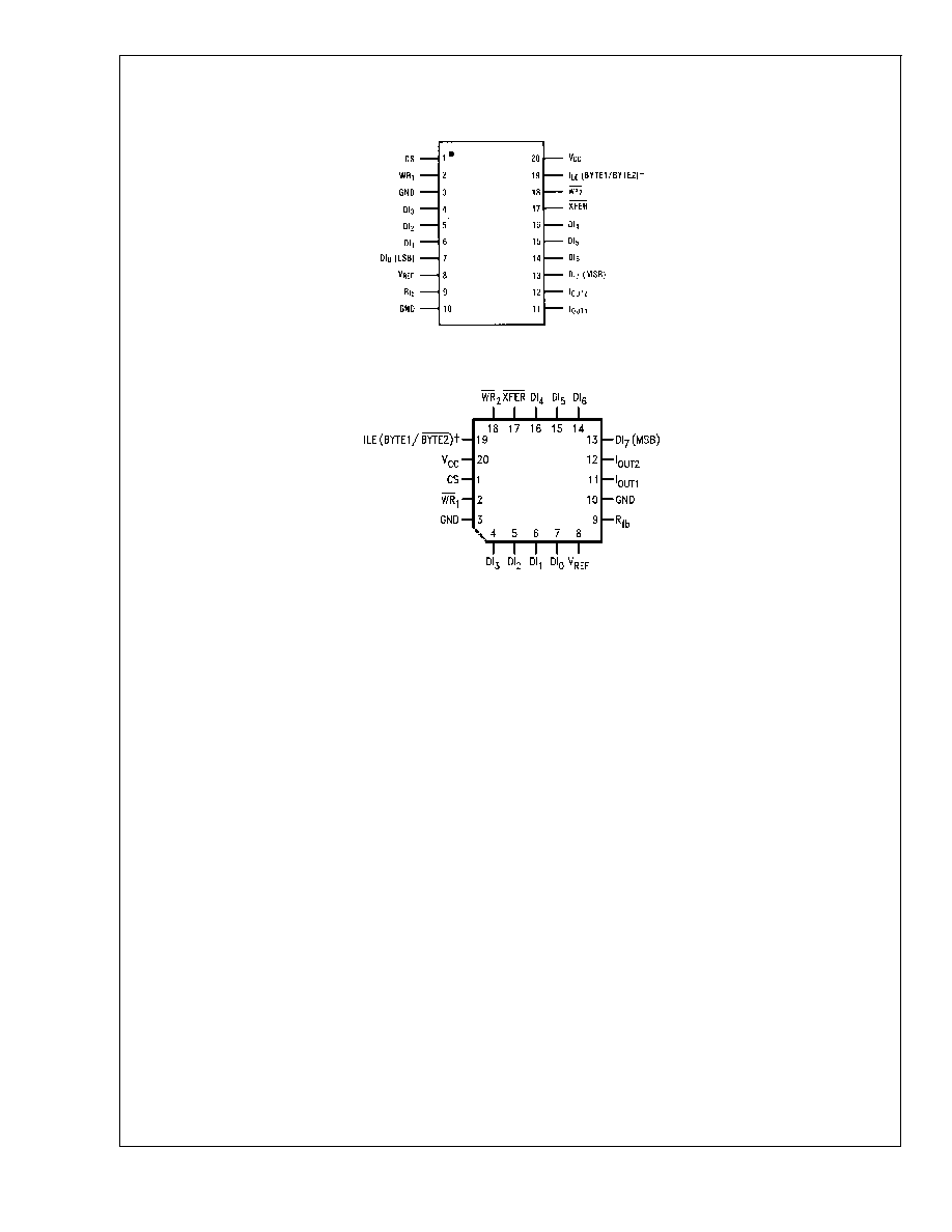
DAC0830/DAC0832
8-Bit µP Compatible, Double-Buffered D to A Converters
General Description
The DAC0830 is an advanced CMOS/Si-Cr 8-bit multiplying
DAC designed to interface directly with the 8080, 8048,
8085, Z80
Æ
, and other popular microprocessors. A deposited
silicon-chromium R-2R resistor ladder network divides the
reference current and provides the circuit with excellent
temperature tracking characteristics (0.05% of Full Scale
Range maximum linearity error over temperature). The cir-
cuit uses CMOS current switches and control logic to
achieve low power consumption and low output leakage
current errors. Special circuitry provides TTL logic input volt-
age level compatibility.
Double buffering allows these DACs to output a voltage
corresponding to one digital word while holding the next
digital word. This permits the simultaneous updating of any
number of DACs.
The DAC0830 series are the 8-bit members of a family of
microprocessor-compatible DACs (MICRO-DAC
TM
).
Features
n
Double-buffered, single-buffered or flow-through digital
data inputs
n
Easy interchange and pin-compatible with 12-bit
DAC1230 series
n
Direct interface to all popular microprocessors
n
Linearity specified with zero and full scale adjust
only -- NOT BEST STRAIGHT LINE FIT.
n
Works with
±
10V reference-full 4-quadrant multiplication
n
Can be used in the voltage switching mode
n
Logic inputs which meet TTL voltage level specs (1.4V
logic threshold)
n
Operates "STAND ALONE" (without µP) if desired
n
Available in 20-pin small-outline or molded chip carrier
package
Key Specifications
n
Current settling time:
1 µs
n
Resolution:
8 bits
n
Linearity:
8, 9, or 10 bits (guaranteed over temp.)
n
Gain Tempco:
0.0002% FS/∞C
n
Low power dissipation:
20 mW
n
Single power supply:
5 to 15 V
DC
Typical Application
00560801
BI-FET
TM
and MICRO-DAC
TM
are trademarks of National Semiconductor Corporation.
Z80
Æ
is a registered trademark of Zilog Corporation.
March 2002
DAC0830/DAC0832
8-Bit
µP
Compatible,
Double-Buffered
D
t
o
A
Converters
© 2002 National Semiconductor Corporation
DS005608
www.national.com
Absolute Maximum Ratings
(Notes 1,
2)
If Military/Aerospace specified devices are required,
please contact the National Semiconductor Sales Office/
Distributors for availability and specifications.
Supply Voltage (V
CC
)
17 V
DC
Voltage at Any Digital Input
V
CC
to GND
Voltage at V
REF
Input
±
25V
Storage Temperature Range
-65∞C to +150∞C
Package Dissipation
at T
A
=25∞C (Note 3)
500 mW
DC Voltage Applied to
I
OUT1
or I
OUT2
(Note 4)
-100 mV to V
CC
ESD Susceptability (Note 4)
800V
Lead Temperature (Soldering, 10 sec.)
Dual-In-Line Package (plastic)
260∞C
Dual-In-Line Package (ceramic)
300∞C
Surface Mount Package
Vapor Phase (60 sec.)
215∞C
Infrared (15 sec.)
220∞C
Operating Conditions
Temperature Range
T
MIN
T
A
T
MAX
Part numbers with "LCN" suffix
0∞C to +70∞C
Part numbers with "LCWM" suffix
0∞C to +70∞C
Part numbers with "LCV" suffix
0∞C to +70∞C
Part numbers with "LCJ" suffix
-40∞C to +85∞C
Part numbers with "LJ" suffix
-55∞C to +125∞C
Voltage at Any Digital Input
V
CC
to GND
Electrical Characteristics
V
REF
=10.000 V
DC
unless otherwise noted. Boldface limits apply over temperature, T
MIN
T
A
T
MAX
. For all other limits
T
A
=25∞C.
Parameter
Conditions
See
Note
V
CC
= 4.75 V
DC
V
CC
= 15.75 V
DC
V
CC
= 5 V
DC
±
5%
V
CC
= 12 V
DC
±
5%
to 15 V
DC
±
5%
Limit
Units
Typ
(Note 12)
Tested
Limit
(Note 5)
Design
Limit
(Note 6)
CONVERTER CHARACTERISTICS
Resolution
8
8
8
bits
Linearity Error Max
Zero and full scale adjusted
4, 8
-10V
V
REF
+10V
DAC0830LJ & LCJ
0.05
0.05
% FSR
DAC0832LJ & LCJ
0.2
0.2
% FSR
DAC0830LCN, LCWM &
LCV
0.05
0.05
% FSR
DAC0831LCN
0.1
0.1
% FSR
DAC0832LCN, LCWM &
LCV
0.2
0.2
% FSR
Differential Nonlinearity
Zero and full scale adjusted
4, 8
Max
-10V
V
REF
+10V
DAC0830LJ & LCJ
0.1
0.1
% FSR
DAC0832LJ & LCJ
0.4
0.4
% FSR
DAC0830LCN, LCWM &
LCV
0.1
0.1
% FSR
DAC0831LCN
0.2
0.2
% FSR
DAC0832LCN, LCWM &
LCV
0.4
0.4
% FSR
Monotonicity
-10V
V
REF
LJ & LCJ
4
8
8
bits
+10V
LCN, LCWM &
LCV
8
8
bits
Gain Error Max
Using Internal R
fb
7
±
0.2
±
1
±
1
% FS
-10V
V
REF
+10V
Gain Error Tempco Max
Using internal R
fb
0.0002
0.0006
%
DAC0830/DAC0832
www.national.com
3
Electrical Characteristics
(Continued)
V
REF
=10.000 V
DC
unless otherwise noted. Boldface limits apply over temperature, T
MIN
T
A
T
MAX
. For all other limits
T
A
=25∞C.
Parameter
Conditions
See
Note
V
CC
= 4.75 V
DC
V
CC
= 15.75 V
DC
V
CC
= 5 V
DC
±
5%
V
CC
= 12 V
DC
±
5%
to 15 V
DC
±
5%
Limit
Units
Typ
(Note 12)
Tested
Limit
(Note 5)
Design
Limit
(Note 6)
CONVERTER CHARACTERISTICS
FS/∞C
Power Supply Rejection
All digital inputs latched high
V
CC
=14.5V to 15.5V
0.0002
0.0025
%
11.5V to 12.5V
0.0006
FSR/V
4.5V to 5.5V
0.013
0.015
Reference
Max
15
20
20
k
Input
Min
15
10
10
k
Output Feedthrough
Error
V
REF
=20 Vp-p, f=100 kHz
All data inputs latched low
3
mVp-p
Output
Leakage
Current Max
I
OUT1
All data inputs LJ & LCJ
10
100
100
nA
latched low
LCN, LCWM &
LCV
50
100
I
OUT2
All data inputs LJ & LCJ
100
100
nA
latched high
LCN, LCWM &
LCV
50
100
Output
I
OUT1
All data inputs
45
pF
Capacitance
I
OUT2
latched low
115
I
OUT1
All data inputs
130
pF
I
OUT2
latched
high
30
DIGITAL AND DC CHARACTERISTICS
Digital Input
Max
Logic Low
LJ:
4.75V
0.6
Voltages
LJ:
15.75V
0.8
LCJ:
4.75V
0.7
V
DC
LCJ:
15.75V
0.8
LCN, LCWM, LCV
0.95
0.8
Min
Logic High
LJ & LCJ
2.0
2.0
V
DC
LCN, LCWM, LCV
1.9
2.0
Digital Input
Max
Digital inputs
<
0.8V
Currents
LJ & LCJ
-50
-200
-200
µA
LCN, LCWM, LCV
-160
-200
µA
Digital inputs
>
2.0V
LJ & LCJ
0.1
+10
+10
µA
LCN, LCWM, LCV
+8
+10
Supply Current
Max
LJ & LCJ
1.2
3.5
3.5
mA
Drain
LCN, LCWM, LCV
1.7
2.0
DAC0830/DAC0832
www.national.com
4
Electrical Characteristics
V
REF
=10.000 V
DC
unless otherwise noted. Boldface limits apply over temperature, T
MIN
T
A
T
MAX
. For all other limits
T
A
=25∞C.
Symbol
Parameter
Conditions
See
Note
V
CC
=15.75 V
DC
V
CC
=12
V
DC
±
5% to 15
V
DC
±
5%
V
CC
=4.75 V
DC
V
CC
=5
V
DC
±
5%
Limit
Units
Typ
(Note 12)
Tested
Limit
(Note 5)
Design Limit
(Note 6)
Typ
(Note 12)
Tested
Limit
(Note 5)
Design
Limit
(Note 6)
AC CHARACTERISTICS
t
s
Current Setting
V
IL
=0V,
V
IH
=5V
1.0
1.0
µs
Time
t
W
Write and XFER
V
IL
=0V,
V
IH
=5V
11
100
250
375
600
Pulse Width Min
9
320
320
900
900
t
DS
Data Setup Time
V
IL
=0V,
V
IH
=5V
9
100
250
375
600
Min
320
320
900
900
t
DH
Data Hold Time
V
IL
=0V,
V
IH
=5V
9
30
50
ns
Min
30
50
t
CS
Control Setup
Time
V
IL
=0V,
V
IH
=5V
9
110
250
600
900
Min
320
320
1100
1100
t
CH
Control Hold Time V
IL
=0V,
V
IH
=5V
9
0
0
10
0
0
Min
0
0
Note 1: Absolute Maximum Ratings indicate limits beyond which damage to the device may occur. DC and AC electrical specifications do not apply when operating
the device beyond its specified operating conditions.
Note 2: All voltages are measured with respect to GND, unless otherwise specified.
Note 3: The maximum power dissipation must be derated at elevated temperatures and is dictated by T
JMAX
,
JA
, and the ambient temperature, T
A
. The maximum
allowable power dissipation at any temperature is P
D
= (T
JMAX
- T
A
)/
JA
or the number given in the Absolute Maximum Ratings, whichever is lower. For this device,
T
JMAX
= 125∞C (plastic) or 150∞C (ceramic), and the typical junction-to-ambient thermal resistance of the J package when board mounted is 80∞C/W. For the N
package, this number increases to 100∞C/W and for the V package this number is 120∞C/W.
Note 4: For current switching applications, both I
OUT1
and I
OUT2
must go to ground or the "Virtual Ground" of an operational amplifier. The linearity error is degraded
by approximately V
OS
˜ V
REF
. For example, if V
REF
= 10V then a 1 mV offset, V
OS
, on I
OUT1
or I
OUT2
will introduce an additional 0.01% linearity error.
Note 5: Tested limits are guaranteed to National's AOQL (Average Outgoing Quality Level).
Note 6: Guaranteed, but not 100% production tested. These limits are not used to calculate outgoing quality levels.
Note 7: Guaranteed at V
REF
=
±
10 V
DC
and V
REF
=
±
1 V
DC
.
Note 8: The unit "FSR" stands for "Full Scale Range." "Linearity Error" and "Power Supply Rejection" specs are based on this unit to eliminate dependence on a
particular V
REF
value and to indicate the true performance of the part. The "Linearity Error" specification of the DAC0830 is "0.05% of FSR (MAX)". This guarantees
that after performing a zero and full scale adjustment (see Sections 2.5 and 2.6), the plot of the 256 analog voltage outputs will each be within 0.05%xV
REF
of a
straight line which passes through zero and full scale.
Note 9: Boldface tested limits apply to the LJ and LCJ suffix parts only.
Note 10: A 100nA leakage current with R
fb
=20k and V
REF
=10V corresponds to a zero error of (100x10
-9
x20x10
3
)x100/10 which is 0.02% of FS.
Note 11: The entire write pulse must occur within the valid data interval for the specified t
W
, t
DS
, t
DH
, and t
S
to apply.
Note 12: Typicals are at 25∞C and represent most likely parametric norm.
Note 13: Human body model, 100 pF discharged through a 1.5 k
resistor.
DAC0830/DAC0832
www.national.com
5