TL H 5690
MICRO-DAC
DAC1208DAC1209DAC1210DAC1230DAC1231DAC1232
12-Bit
m
P
Compatible
Double-Buffered
D
t
o
A
Converters
February 1995
MICRO-DAC
TM
DAC1208 DAC1209 DAC1210 DAC1230
DAC1231 DAC1232 12-Bit mP Compatible
Double-Buffered D to A Converters
General Description
The DAC1208 and the DAC1230 series are 12-bit multiply-
ing D to A converters designed to interface directly with a
wide variety of microprocessors (8080 8048 8085 Z-80
etc ) Double buffering input registers and associated con-
trol lines allow these DACs to appear as a two-byte ``stack''
in the system's memory or I O space with no additional in-
terfacing logic required
The DAC1208 series provides all 12 input lines to allow sin-
gle buffering for maximum throughput when used with 16-bit
processors These input lines can also be externally config-
ured to permit an 8-bit data interface The DAC1230 series
can be used with an 8-bit data bus directly as it internally
formulates the 12-bit DAC data from its 8 input lines All of
these DACs accept left-justified data from the processor
The analog section is a precision silicon-chromium (Si-Cr)
R-2R ladder network and twelve CMOS current switches
An inverted R-2R ladder structure is used with the binary
weighted currents switched between the I
OUT1
and I
OUT2
maintaining a constant current in each ladder leg indepen-
dent of the switch state Special circuitry provides TTL logic
input voltage level compatibility
The DAC1208 series and DAC1230 series are the 12-bit
members of a family of microprocessor compatible DACs
(MICRO-DACs
TM
) For applications requiring other resolu-
tions the DAC1000 series for 10-bit and DAC0830 series
for 8-bit are available alternatives
Features
Y
Linearity specified with zero and full-scale adjust only
Y
Direct interface to all popular microprocessors
Y
Double-buffered single-buffered or flow through digital
data inputs
Y
Logic inputs which meet TTL voltage level specs (1 4V
logic threshold)
Y
Works with
g
10V reference
full 4-quadrant
multiplication
Y
Operates stand-alone (without mP) if desired
Y
All parts guaranteed 12-bit monotonic
Y
DAC1230 series is pin compatible with the DAC0830
series 8-bit MICRO-DACs
Key Specifications
Y
Current Settling Time
1 ms
Y
Resolution
12 Bits
Y
Linearity (Guaranteed
over temperature)
10 11 or 12 Bits of FS
Y
Gain Tempco
1 3 ppm C
Y
Low Power Dissipation
20 mW
Y
Single Power Supply
5 V
DC
to 15 V
DC
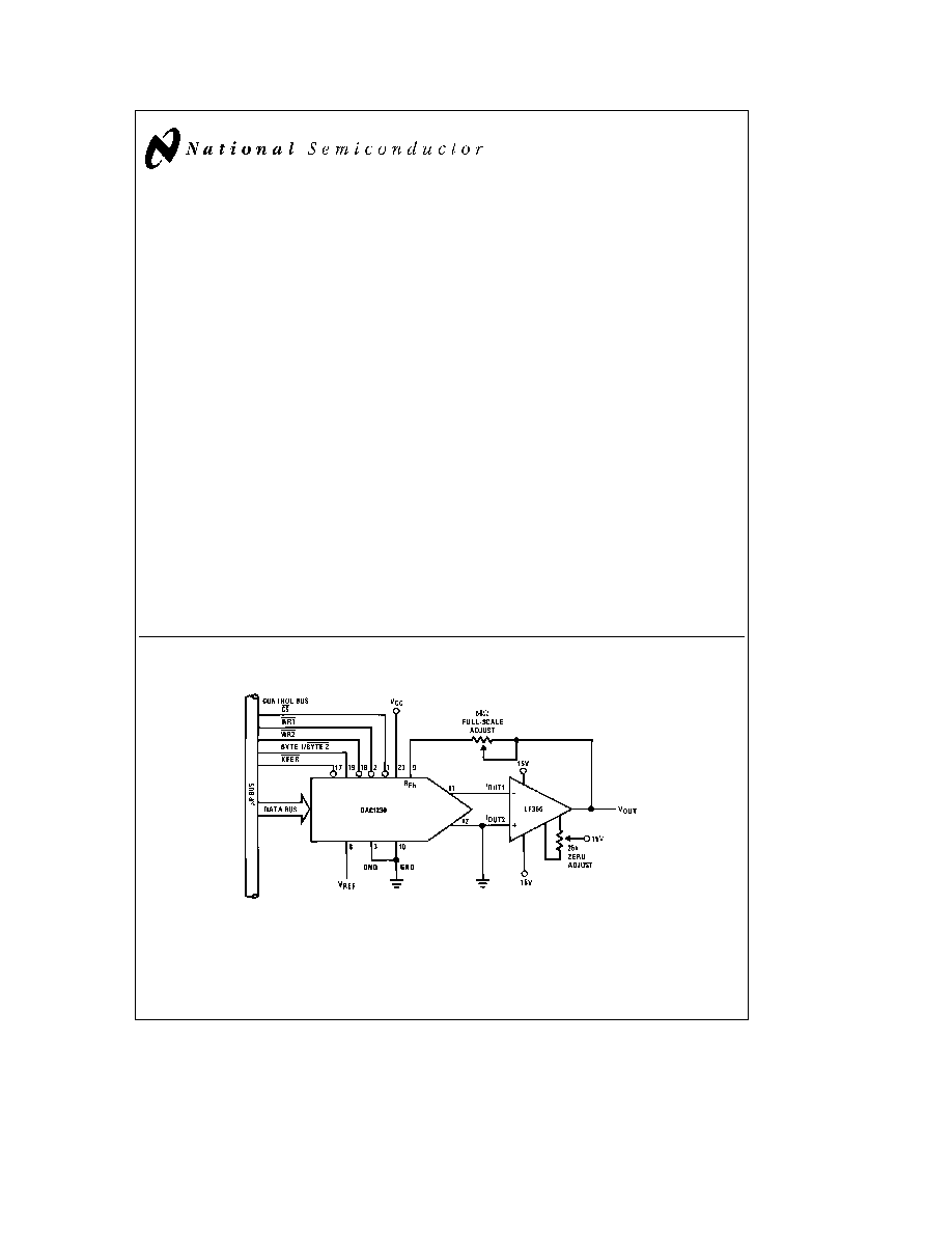
Typical Application
TL H 5690 ≠ 1
TRI-STATE
is a registered trademark of National Semiconductor Corp
MICRO-DAC
TM
is a trademark of National Semiconductor Corp
C1995 National Semiconductor Corporation
RRD-B30M115 Printed in U S A
Absolute Maximum Ratings
If Military Aerospace specified devices are required
please contact the National Semiconductor Sales
Office Distributors for availability and specifications
(Notes 1 and 2)
Supply Voltage (V
CC
)
17 V
DC
Voltage at Any Digital Input
V
CC
to GND
Voltage at V
REF
Input
g
25V
Storage Temperature Range
b
65 C to
a
150 C
Package Dissipation at T
A
e
25 C
500 mW
(Note 3)
DC Voltage Applied to I
OUT1
or I
OUT2
(Note 4)
b
100 mV to V
CC
ESD Susceptability
800V
Operating Conditions
Lead Temperature (Soldering 10 sec )
300 C
Temperature Range
T
MIN
s
T
A
s
T
MAX
DAC1208LCJ DAC1209LCJ
DAC1210LCJ DAC1230LCJ
DAC1231LCJ DAC1232LCJ
DAC1231LIN DAC1232LIN
b
40 C
s
T
A
s
a
85 C
DAC1208LCJ-1 DAC1210LCJ-1
DAC1230LCJ-1 DAC1231LCJ-1
DAC1232LCJ-1 DAC1231LCN
DAC1232LCN DAC1231LCWM
DAC1232LCWM
0 C
s
T
A
s
a
70 C
Range of V
CC
4 75 V
DC
to 16 V
DC
Voltage at Any Digital Input
V
CC
to GND
Electrical Characteristics
V
REF
e
10 000 V
DC
V
CC
e
11 4 V
DC
to 15 75 V
DC
unless otherwise noted Boldface limits apply from T
MIN
to T
MAX
(see
Note 13)
all other limits T
A
e
T
J
e
25 C
Typ
Tested
Design
Parameter
Conditions
Notes
(Note 10)
Limit
Limit
Units
(Note 5)
(Note 6)
Resolution
12
12
12
Bits
Linearity Error
Zero and Full-Scale
4 7 13
(End Point Linearity)
Adjusted
DAC1208 DAC1230
g
0 018
g
0 018
% of FSR
DAC1209 DAC1231
g
0 024
g
0 024
% of FSR
DAC1210 DAC1232
g
0 050
g
0 05
% of FSR
Differential Non-Linearity
Zero and Full-Scale
4 7 13
Adjusted
DAC1208 DAC1230
g
0 018
g
0 018
% of FSR
DAC1209 DAC1231
g
0 024
g
0 024
% of FSR
DAC1210 DAC1232
g
0 050
g
0 05
% of FSR
Monotonicity
4
12
12
12
Bits
Gain Error (Min)
Using Internal R
Fb
7
b
0 1
0 0
% of FSR
Gain Error (Max)
V
ref
e
g
10V
g
1V
7
b
0 1
b
0 2
% of FSR
Gain Error Tempco
7
g
1 3
g
6 0
ppm of FS C
Power Supply Rejection
All Digital Inputs
7
g
3 0
g
30
ppm of FSR V
Latched High
Reference Input Resistance (Min)
13
15
10
10
kX
Reference Input Resistance (Max)
15
20
20
Output Feedthrough Error
V
REF
e
20 Vp-p f
e
100 kHz
All Data Inputs Latched
9
3 0
mVp-p
Low
Output Capacitance
All Data Inputs
I
OUT1
200
pF
Latched High
I
OUT2
70
pF
All Data Inputs
I
OUT1
70
pF
Latched Low
I
OUT2
200
pF
Supply Current Drain
13
2 0
2 5
mA
Output Leakage Current
I
OUT1
All Data Inputs Latched
11 13
0 1
15
15
nA
Low
I
OUT2
All Data Inputs Latched
11 13
0 1
15
15
nA
High
Digital Input Threshold
Low Threshold
13
0 8
0 8
V
DC
High Threshold
13
2 2
2 2
V
DC
Digital Input Currents
Digital Inputs
k
0 8V
13
b
200
b
200
m
A
DC
Digital Inputs
l
2 2V
13
10
10
m
A
DC
2

Electrical Characteristics
(Continued)
V
REF
e
10 000 V
DC
V
CC
e
11 4 V
DC
to 15 75 V
DC
unless otherwise noted Boldface limits apply from T
MIN
to T
MAX
(see
Note 13)
all other limits T
A
e
T
J
e
25 C
See
Typ
Tested
Design
Symbol
Parameter
Conditions
Note
(Note 10)
Limit
Limit
Units
(Note 5)
(Note 6)
AC CHARACTERISTICS
t
s
Current Setting Time
V
IL
e
0V V
IH
e
5V
1 0
m
s
t
W
Write and XFER
V
IL
e
0V V
IH
e
5V
8
50
320
Pulse Width Min
320
t
DS
Data Setup Time Min
V
IL
e
0V V
IH
e
5V
70
320
320
t
DH
Data Hold Time Min
V
IL
e
0V V
IH
e
5V
30
90
ns
90
t
CS
Control Setup Time Min
V
IL
e
0V V
IH
e
5V
60
320
320
t
CH
Control Hold Time Min
V
IL
e
0V V
IH
e
5V
0
10
Note 1
Absolute Maximum Ratings indicate limits beyond which damage to the device may occur DC and AC electrical specifications do not apply when operating
the device beyond its specified operating conditions
Note 2
All voltages are measured with respect to GND unless otherwise specified
Note 3
This 500 mW specification applies for all packages The low intrinsic power dissipation of this part (and the fact that there is no way to significantly modify
the power dissipation) removes concern for heat sinking
Note 4
Both I
OUT1
and I
OUT2
must go to ground or the virtual ground of an operational amplifier The linearity error is degraded by approximately V
OS
d
V
REF
For
example if V
REF
e
10V then a 1 mV offset V
OS
on I
OUT1
or I
OUT2
will introduce an additional 0 01% linearity error
Note 5
Tested and guaranteed to National's AOQL (Average Outgoing Quality Level)
Note 6
Design limits are guaranteed but not 100% tested These limits are not used to calculate outgoing quality levels Guaranteed for V
CC
e
11 4V to 15 75V
and V
REF
e b
10V to
a
10V
Note 7
The unit FSR stands for full-scale range Linearity Error and Power Supply Rejection specs are based on this unit to eliminate dependence on a particular
V
REF
value to indicate the true performance of the part The Linearity Error specification of the DAC1208 is 0 012% of FSR(max) This guarantees that after
performing a zero and full-scale adjustment the plot of the 4096 analog voltage outputs will each be within 0 012%
c
V
REF
of a straight line which passes through
zero and full-scale The unit ppm of FSR(parts per million of full-scale range) and ppm of FS(parts per million of full-scale) are used for convenience to define specs
of very small percentage values typical of higher accuracy converters In this instance 1 ppm of FSR
e
V
REF
10
6
is the conversion factor to provide an actual
output voltage quantity For example the gain error tempco spec of
g
6 ppm of FS C represents a worst-case full-scale gain error change with temperature from
b
40 C to
a
85 C of
g
(6)(V
REF
10
6
)(125 C) or
g
0 75 (10
b
3
) V
REF
which is
g
0 075% of V
REF
Note 8
This spec implies that all parts are guaranteed to operate with a write pulse or transfer pulse width (t
W
) of 320 ns A typical part will operate with t
W
of only
100 ns The entire write pulse must occur within the valid data interval for the specified t
W
t
DS
t
DH
and t
S
to apply
Note 9
To achieve this low feedthrough in the D package the user must ground the metal lid If the lid is left floating the feedthrough is typically 6 mV
Note 10
Typicals are at 25 C and represent the most likely parametric norm
Note 11
A 10 nA leakage current with R
Fb
e
20k and V
REF
e
10V corresponds to a zero error of (10
c
10
b
9c
20
c
10
3
)
c
100% 10V or 0 002% of FS
Note 12
Human body model 100 pF discharged through a 1 5 kX resistor
Note 13
Tested limit for
b
1 suffix parts applies only at 25 C
Connection Diagrams
Dual-In-Line Package
Dual-In-Line Package
TL H 5690 ≠ 2
See Ordering Information
3

Switching Waveforms
TL H 5690 ≠ 3
Typical Performance Characteristics
Digital Input Threshold
vs V
CC
Digital Input Threshold vs
Temperature
Gain and Linearity Error
Variation vs Temperature
Gain and Linearity Error
Variation vs Supply Voltage
Control Set-Up Time t
CS
Data Hold Time t
DH
Write Pulse Width t
W
Data Set-Up Time t
DS
TL H 5690 ≠ 4
4

Definition of Package Pinouts
CONTROL SIGNALS
(all control signals are level actuated)
CS
Chip Select (active low) The CS will enable WR1
WR1
Write 1 The active low WR1 is used to load the digital
data bits (DI) into the input latch The data in the input latch
is latched when WR1 is high The 12-bit input latch is split
into two latches One holds the first 8 bits while the other
holds 4 bits The Byte 1 Byte 2 control pin is used to select
both latches when Byte 1 Byte 2 is high or to overwrite the
4-bit input latch when in the low state
Byte 1 Byte 2
Byte Sequence Control When this control is
high all 12 locations of the input latch are enabled When
low only the four least significant locations of the input latch
are enabled
WR2
Write 2 (active low) The WR2 will enable XFER
XFER
Transfer Control Signal (active low) This signal in
combination with WR2 causes the 12-bit data which is
available in the input latches to transfer to the DAC register
DI
0
to DI
11
Digital Inputs DI
0
is the least significant digital
input (LSB) and DI
11
is the most significant digital input
(MSB)
I
OUT1
DAC Current Output 1 I
OUT1
is a maximum for a
digital code of all 1s in the DAC register and is zero for all
0s in the DAC register
I
OUT2
DAC Current Output 2 I
OUT2
is a constant minus
I
OUT1
or I
OUT1
a
I
OUT2
e
constant (for a fixed reference
voltage) This constant current is
V
REF
c
1
b
1
4096
J
divided by the reference input resistance
R
Fb
Feedback Resistor The feedback resistor is provided
on the IC chip for use as the shunt feedback resistor for the
external op amp which is used to provide an output voltage
for the DAC This on-chip resistor should always be used
(not an external resistor) since it matches the resistors in
the on-chip R-2R ladder and tracks these resistors over
temperature
V
REF
Reference Voltage Input This input connects an ex-
ternal precision voltage source to the internal R-2R ladder
V
REF
can be selected over the range of 10V to
b
10V This
is also the analog voltage input for a 4-quadrant multiplying
DAC application
V
CC
Digital Supply Voltage This is the power supply pin for
the part V
CC
can be from 5 V
DC
to 15 V
DC
Operation is
optimum for 15 V
DC
GND
Pins 3 and 12 of the DAC1208 DAC1209 and
DAC1210 must be connected to ground Pins 3 and 10 of
the DAC1230 DAC1231 and DAC1232 must be connected
to ground It is important that I
OUT1
and I
OUT2
are at ground
potential for current switching applications Any difference
of potential (V
OS
on these pins) will result in a linearity
change of
V
OS
3 V
REF
For example if V
REF
e
10V and these ground pins are 9
mV offset from I
OUT1
and I
OUT2
the linearity change will be
0 03%
Definition of Terms
Resolution
Resolution is defined as the reciprocal of the
number of discrete steps in the DAC output It is directly
related to the number of switches or bits within the DAC For
example the DAC1208 has 2
12
or 4096 steps and therefore
has 12-bit resolution
Linearity Error
Linearity error is the maximum deviation
from a
straight line passing through the endpoints of the
DAC transfer characteristic It is measured after adjusting
for zero and full-scale Linearity error is a parameter intrinsic
to the device and cannot be externally adjusted
National's linearity test (a) and the best straight line test (b)
used by other suppliers are illustrated below The best
straight line (b) requires a special zero and FS adjustment
for each part which is almost impossible for the user to
determine The end point test uses a standard zero FS ad-
justment procedure and is a much more stringent test for
DAC linearity
Power Supply Sensitivity
Power supply sensitivity is a
measure of the effect of power supply changes on the DAC
full-scale output
Settling Time
Full-scale current settling time requires zero
to full-scale or full-scale to zero output change Settling time
is the time required from a code transition until the DAC
output reaches within
g
LSB of the final output value
Full-Scale Error
Full-scale error is a measure of the output
error between an ideal DAC and the actual device output
Ideally for the DAC1208 or DAC1230 series full-scale is
V
REF
b
1 LSB
For V
REF
e
10V and unipolar operation
V
FULL-SCALE
e
10 0000V
b
2 44 mV
e
9 9976V
Full-scale
error is adjustable to zero
Differential Non-Linearity
The difference between any
two consecutive codes in the transfer curve from the theo-
retical 1 LSB is differential non-linearity
Monotonic
If the output of a DAC increases for increasing
digital input code then the DAC is monotonic A 12-bit DAC
which is monotonic to 12 bits simply means that input in-
creasing digital input codes will produce an increasing ana-
log output
TL H 5690 ≠ 5
a) End Point Test After Zero
and FS Adjust
b) Shifting FS Adjust to Pass
Best Straight Line Test
5