DAC121S101
12-Bit Micro Power Digital-to-Analog Converter with
Rail-to-Rail Output
General Description
The DAC121S101 is a full-featured, general purpose 12-bit
voltage-output digital-to-analog converter (DAC) that can
operate from a single +2.7V to 5.5V supply and consumes
just 177 µA of current at 3.6 Volts. The on-chip output
amplifier allows rail-to-rail output swing and the three wire
serial interface operates at clock rates up to 30 MHz over the
specified supply voltage range and is compatible with stan-
dard SPI
TM
, QSPI, MICROWIRE and DSP interfaces. Com-
petitive devices are limited to 20 MHz clock rates at supply
voltages in the 2.7V to 3.6V range.
The supply voltage for the DAC121S101 serves as its volt-
age reference, providing the widest possible output dynamic
range. A power-on reset circuit ensures that the DAC output
powers up to zero volts and remains there until there is a
valid write to the device. A power-down feature reduces
power consumption to less than a microWatt.
The low power consumption and small packages of the
DAC121S101 make it an excellent choice for use in battery
operated equipment.
The DAC121S101 is a direct replacement for the AD5320
and the DAC7512 and is one of a family of pin compatible
DACs, including the 8-bit DAC081S101 and the 10-bit
DAC101S101. The DAC121S101 operates over the ex-
tended industrial temperature range of -40∞C to +105∞C.
Features
n
Guaranteed Monotonicity
n
Low Power Operation
n
Rail-to-Rail Voltage Output
n
Power-on Reset to Zero Volts Output
n
SYNC Interrupt Facility
n
Wide power supply range (+2.7V to +5.5V)
n
Small Packages
n
Power Down Feature
Key Specifications
n
Resolution
12 bits
n
DNL
+0.25, -0.15 LSB (typ)
n
Output Settling Time
8 µs (typ)
n
Zero Code Error
4 mV (typ)
n
Full-Scale Error
-0.06 %FS (typ)
n
Power Consumption
-- Normal Mode
0.64mW (3.6V) / 1.43mW (5.5V) typ
-- Pwr Down Mode
0.14µW (3.6V) / 0.39µW (5.5V) typ
Applications
n
Battery-Powered Instruments
n
Digital Gain and Offset Adjustment
n
Programmable Voltage & Current Sources
n
Programmable Attenuators
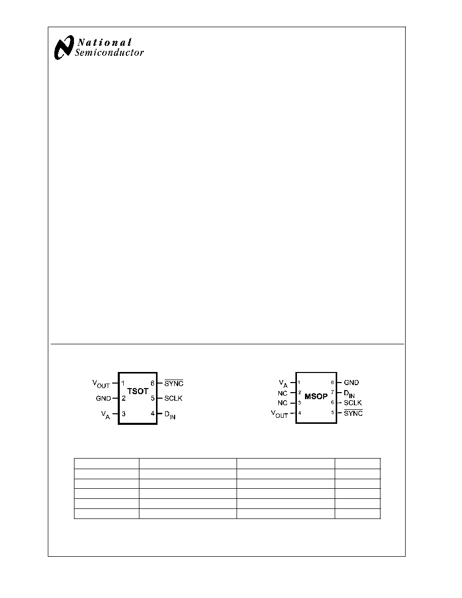
Pin Configuration
20114901
20114902
Ordering Information
Order Numbers
Temperature Range
Package
Top Mark
DAC121S101CIMM
-40∞C
T
A
+105∞C
MSOP
X60C
DAC121S101CIMMX
-40∞C
T
A
+105∞C
MSOP Tape-and-Reel
X60C
DAC121S101CIMK
-40∞C
T
A
+105∞C
TSOT
X61C
DAC121S101CIMKX
-40∞C
T
A
+105∞C
TSOT Tape-and-Reel
X61C
DAC121S101EVAL
Evaluation Board
SPI
TM
is a trademark of Motorola, Inc.
June 2005
DAC121S101
12-Bit
Micro
Power
Digital-to-Analog
Converter
with
Rail-to-Rail
Output
© 2005 National Semiconductor Corporation
DS201149
www.national.com

Block Diagram
20114903
Pin Descriptions
TSOT
(SOT-23)
Pin No.
MSOP
Pin No.
Symbol
Description
1
4
V
OUT
DAC Analog Output Voltage.
2
8
GND
Ground reference for all on-chip circuitry.
3
1
V
A
Power supply and Reference input. Should be decoupled
to GND.
4
7
D
IN
Serial Data Input. Data is clocked into the 16-bit shift
register on the falling edges of SCLK after the fall of
SYNC.
5
6
SCLK
Serial Clock Input. Data is clocked into the input shift
register on the falling edges of this pin.
6
5
SYNC
Frame synchronization input for the data input. When this
pin goes low, it enables the input shift register and data
is transferred on the falling edges of SCLK. The DAC is
updated on the 16th clock cycle unless SYNC is brought
high before the 16th clock, in which case the rising edge
of SYNC acts as an interrupt and the write sequence is
ignored by the DAC.
2, 3
NC
No Connect. There is no internal connection to these
pins.
DAC121S101
www.national.com
2
Absolute Maximum Ratings
(Notes 1, 2)
If Military/Aerospace specified devices are required,
please contact the National Semiconductor Sales Office/
Distributors for availability and specifications.
Supply Voltage, V
A
6.5V
Voltage on any Input Pin
-0.3V to (V
A
+ 0.3V)
Input Current at Any Pin (Note 3)
10 mA
Package Input Current (Note 3)
20 mA
Power Consumption at T
A
= 25∞C
See (Note 4)
ESD Susceptibility (Note 5)
Human Body Model
Machine Model
2500V
250V
Soldering Temperature, Infrared,
10 Seconds (Note 6)
235∞C
Storage Temperature
-65∞C to +150∞C
Operating Ratings
(Notes 1, 2)
Operating Temperature Range
-40∞C
T
A
+105∞C
Supply Voltage, V
A
+2.7V to 5.5V
Any Input Voltage (Note 7)
-0.1 V to (V
A
+ 0.1 V)
Output Load
0 to 1500 pF
SCLK Frequency
Up to 30 MHz
Package Thermal Resistances
Package
JA
8-Lead MSOP
240∞C/W
6-Lead TSOT
250∞C/W
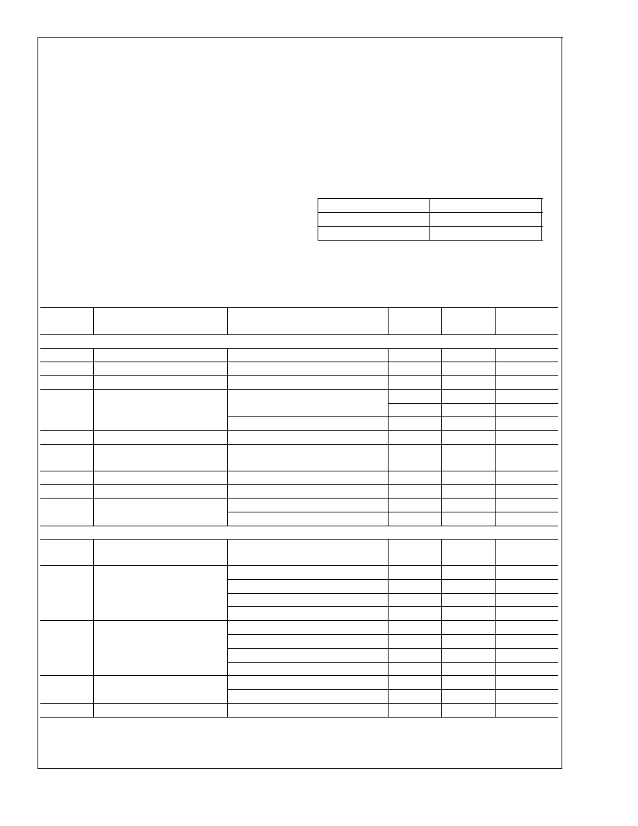
Electrical Characteristics
Values shown in this table are design targets and are subject to change before product release. The following specifica-
tions apply for V
A
= +2.7V to +5.5V, R
L
= 2k
to GND, C
L
= 200 pF to GND, f
SCLK
= 30 MHz, input code range 48 to 4047.
Boldface limits apply for T
MIN
T
A
T
MAX
: all other limits T
A
= 25∞C, unless otherwise specified.
Symbol
Parameter
Conditions
Typical
(Note 9)
Limits
(Note 9)
Units
(Limits)
STATIC PERFORMANCE
Resolution
12
Bits (min)
Monotonicity
12
Bits (min)
INL
Integral Non-Linearity
Over Decimal codes 48 to 4047
±
2.6
±
8
LSB (max)
DNL
Differential Non-Linearity
V
A
= 2.7V to 5.5V
+0.25
+1.0
LSB (max)
-0.15
-0.7
LSB (min)
V
A
= 4.5V to 5.5V (Note 10)
±
0.11
±
0.5
LSB (max)
ZE
Zero Code Error
I
OUT
= 0
+4
+15
mV (max)
FSE
Full-Scale Error
I
OUT
= 0
-0.06
-1.0
%FSR
(max)
GE
Gain Error
All ones Loaded to DAC register
-0.10
±
1.0
%FSR
ZCED
Zero Code Error Drift
-20
µV/∞C
TC GE
Gain Error Tempco
V
A
= 3V
-0.7
ppm/∞C
V
A
= 5V
-1.0
ppm/∞C
OUTPUT CHARACTERISTICS
Output Voltage Range
(Note 10)
0
V
A
V (min)
V (max)
ZCO
Zero Code Output
V
A
= 3V, I
OUT
= 10 µA
1.8
mV
V
A
= 3V, I
OUT
= 100 µA
5.0
mV
V
A
= 5V, I
OUT
= 10 µA
3.7
mV
V
A
= 5V, I
OUT
= 100 µA
5.4
mV
FSO
Full Scale Output
V
A
= 3V, I
OUT
= 10 µA
2.997
V
V
A
= 3V, I
OUT
= 100 µA
2.990
V
V
A
= 5V, I
OUT
= 10 µA
4.995
V
V
A
= 5V, I
OUT
= 100 µA
4.992
V
Maximum Load Capacitance
R
L
=
1500
pF
R
L
= 2k
1500
pF
DC Output Impedance
1.3
Ohm
DAC121S101
www.national.com
3

Electrical Characteristics
(Continued)
Values shown in this table are design targets and are subject to change before product release. The following specifica-
tions apply for V
A
= +2.7V to +5.5V, R
L
= 2k
to GND, C
L
= 200 pF to GND, f
SCLK
= 30 MHz, input code range 48 to 4047.
Boldface limits apply for T
MIN
T
A
T
MAX
: all other limits T
A
= 25∞C, unless otherwise specified.
Symbol
Parameter
Conditions
Typical
(Note 9)
Limits
(Note 9)
Units
(Limits)
I
OS
Output Short Circuit Current
V
A
= 5V, V
OUT
= 0V,
Input code = FFFh
-63
mA
V
A
= 3V, V
OUT
= 0V,
Input code = FFFh
-50
mA
V
A
= 5V, V
OUT
= 5V,
Input code = 000h
74
mA
V
A
= 3V, V
OUT
= 3V,
Input code = 000h
53
mA
LOGIC INPUT
I
IN
Input Current (Note 10)
±
1
µA (max)
V
IL
Input Low Voltage (Note 10)
V
A
= 5V
0.8
V (max)
V
A
= 3V
0.5
V (max)
V
IH
Input High Voltage (Note 10)
V
A
= 5V
2.4
V (min)
V
A
= 3V
2.1
V (min)
C
IN
Input Capacitance (Note 10)
3
pF (max)
POWER REQUIREMENTS
I
A
Supply Current (output
unloaded)
Normal Mode
f
SCLK
= 30 MHz
V
A
= 5.5V
260
312
µA (max)
V
A
= 3.6V
177
217
µA (max)
Normal Mode
f
SCLK
= 20 MHz
V
A
= 5.5V
224
279
µA (max)
V
A
= 3.6V
158
197
µA (max)
Normal Mode
f
SCLK
= 0
V
A
= 5.5V
153
µA (max)
V
A
= 3.6V
118
µA (max)
All PD Modes,
f
SCLK
= 30 MHz
V
A
= 5.0V
84
µA (max)
V
A
= 3.0V
42
µA (max)
All PD Modes,
f
SCLK
= 20 MHz
V
A
= 5.0V
56
µA (max)
V
A
= 3.0V
28
µA (max)
All PD Modes,
f
SCLK
= 0 (Note 10)
V
A
= 5.5V
0.07
1.0
µA (max)
V
A
= 3.6V
0.04
1.0
µA (max)
P
C
Power Consumption (output
unloaded)
Normal Mode
f
SCLK
= 30 MHz
V
A
= 5.5V
1.43
1.72
mW (max)
V
A
= 3.6V
0.64
0.78
mW (max)
Normal Mode
f
SCLK
= 20 MHz
V
A
= 5.5V
1.23
1.53
mW (max)
V
A
= 3.6V
0.57
0.71
mW (max)
Normal Mode
f
SCLK
= 0
V
A
= 5.5V
0.84
µW (max)
V
A
= 3.6V
0.42
µW (max)
All PD Modes,
f
SCLK
= 30 MHz
V
A
= 5.0V
0.42
µW (max)
V
A
= 3.0V
0.13
µW (max)
All PD Modes,
f
SCLK
= 20 MHz
V
A
= 5.0V
0.28
µW (max)
V
A
= 3.0V
0.08
µW (max)
All PD Modes,
f
SCLK
= 0 (Note 10)
V
A
= 5.5V
0.39
5.5
µW (max)
V
A
= 3.6V
0.14
3.6
µW (max)
I
OUT
/ I
A
Power Efficiency
I
LOAD
= 2mA
V
A
= 5V
91
%
V
A
= 3V
94
%
DAC121S101
www.national.com
4

A.C. and Timing Characteristics
Values shown in this table are design targets and are subject to change before product release. The following specifica-
tions apply for V
A
= +2.7V to +5.5V, R
L
= 2k
to GND, C
L
= 200 pF to GND, f
SCLK
= 30 MHz, input code range 48 to 4047.
Boldface limits apply for T
MIN
T
A
T
MAX
: all other limits T
A
= 25∞C, unless otherwise specified.
Symbol
Parameter
Conductions
Typical
Limits
Units
(Limits)
f
SCLK
SCLK Frequency
30
MHz (max)
t
s
Output Voltage Settling Time
(Note 10)
400h to C00h code
change, R
L
= 2k
C
L
200 pF
8
10
µs (max)
C
L
= 500 pF
12
µs
00Fh to FF0h code
change, R
L
= 2k
C
L
200 pF
8
µs
C
L
= 500 pF
12
µs
SR
Output Slew Rate
1
V/µs
Glitch Impulse
Code change from 800h to 7FFh
12
nV-sec
Digital Feedthrough
0.5
nV-sec
t
WU
Wake-Up Time
V
A
= 5V
1.6
µs
V
A
= 3V
1.9
µs
1/f
SCLK
SCLK Cycle Time
33
ns (min)
t
H
SCLK High time
5
13
ns (min)
t
L
SCLK Low Time
5
13
ns (min)
t
SUCL
Set-up Time SYNC to SCLK Rising
Edge
-15
0
ns (min)
t
SUD
Data Set-Up Time
2.5
5
ns (min)
t
DHD
Data Hold Time
2.5
4.5
ns (min)
t
CS
SCLK fall to rise of SYNC
V
A
= 5V
0
3
ns (min)
V
A
= 3V
-2
1
ns (min)
t
SYNC
SYNC High Time
2.7
V
A
3.6
9
20
ns (min)
3.6
V
A
5.5
5
10
ns (min)
Note 1: Absolute Maximum Ratings indicate limits beyond which damage to the device may occur. Operating Ratings indicate conditions for which the device is
functional, but do not guarantee specific performance limits. For guaranteed specifications and test conditions, see the Electrical Characteristics. The guaranteed
specifications apply only for the test conditions listed. Some performance characteristics may degrade when the device is not operated under the listed test
conditions.
Note 2: All voltages are measured with respect to GND = 0V, unless otherwise specified
Note 3: When the input voltage at any pin exceeds the power supplies (that is, less than GND, or greater than V
A
), the current at that pin should be limited to 10
mA. The 20 mA maximum package input current rating limits the number of pins that can safely exceed the power supplies with an input current of 10 mA to two.
Note 4: The absolute maximum junction temperature (T
J
max) for this device is 150∞C. The maximum allowable power dissipation is dictated by T
J
max, the
junction-to-ambient thermal resistance (
JA
), and the ambient temperature (T
A
), and can be calculated using the formula P
D
MAX = (T
J
max - T
A
) /
JA
. The values
for maximum power dissipation will be reached only when the device is operated in a severe fault condition (e.g., when input or output pins are driven beyond the
power supply voltages, or the power supply polarity is reversed). Obviously, such conditions should always be avoided.
Note 5: Human body model is 100 pF capacitor discharged through a 1.5 k
resistor. Machine model is 220 pF discharged through ZERO Ohms.
Note 6: See the section entitled "Surface Mount" found in any post 1986 National Semiconductor Linear Data Book for methods of soldering surface mount devices.
Note 7: The analog inputs are protected as shown below. Input voltage magnitudes up to V
A
+ 300 mV or to 300 mV below GND will not damage this device.
However, errors in the conversion result can occur if any input goes above V
A
or below GND by more than 100 mV. For example, if V
A
is 2.7V
DC
, ensure that -100mV
input voltages 2.8V
DC
to ensure accurate conversions.
20114904
Note 8: To guarantee accuracy, it is required that V
A
be well bypassed.
Note 9: Typical figures are at T
J
= 25∞C, and represent most likely parametric norms. Test limits are guaranteed to National's AOQL (Average Outgoing Quality
Level).
Note 10: This parameter is guaranteed by design and/or characterization and is not tested in production.
DAC121S101
www.national.com
5