TL K 10124
DH0035DH0035C
PIN
Diode
Driver
February 1995
DH0035 DH0035C
PIN Diode Driver
General Description
The DH0035 DH0035C is a high speed digital driver de-
signed to drive PIN diodes in RF modulators and switches
The device is used in conjunction with an input buffer such
as the DM7830 DM8830 or DM5440 DM7440
Features
Y
Large output voltage swing
30V
Y
Peak output current in excess of 1A
Y
Inputs TTL DTL compatible
Y
Short propagation delay
10 ns
Y
High repetition rate
5 MHz
The DH0035 DH0035C is capable of driving a variety of PIN
diode types including parallel serial anode grounded and
cathode grounded For additional information see
AN-49
PIN Diode Drivers
The DH0035 is guaranteed over the temperature range
b
55 C to
a
125 C whereas the DH0035C is guaranteed
from 0 C to
a
85 C
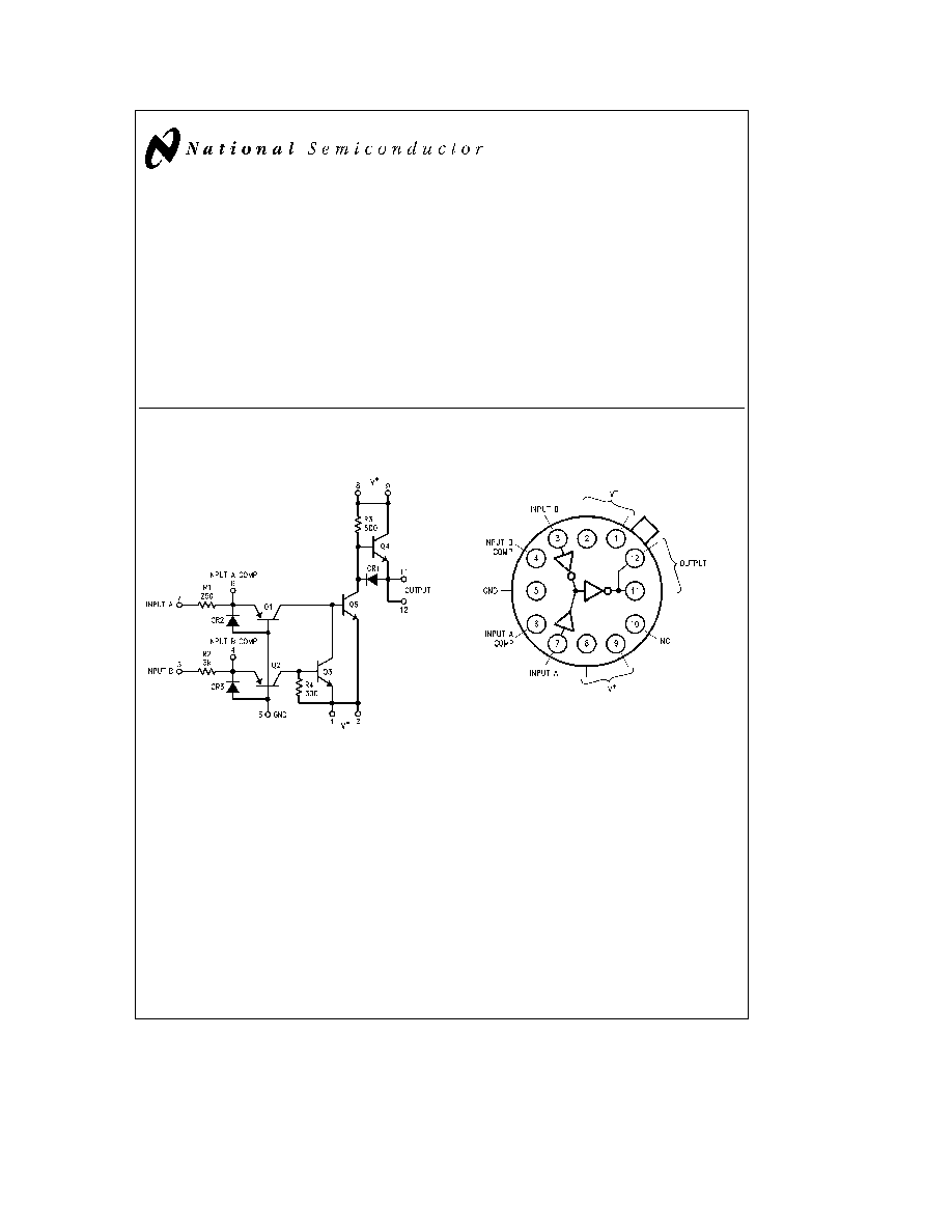
Schematic and Connection Diagrams
TL K 10124 � 1
Metal Can Package
TL K 10124 � 2
Top View
Order Number DH0035G-MIL or DH0035CG
See NS Package Number G12B
C1995 National Semiconductor Corporation
RRD-B30M115 Printed in U S A
Absolute Maximum Ratings
If Military Aerospace specified devices are required
please contact the National Semiconductor Sales
Office Distributors for availability and specifications
V
b
Supply Voltage Differential (Pin 5 to Pin 1 or 2)
40V
V
a
Supply Voltage Differential (Pin 1 or 2 to Pin 8 or 9) 30V
Input Current (Pin 3 or 7)
g
75 mA
Peak Output Current
g
1 0A
Power Dissipation (Note 3)
1 5W
Storage Temperature Range
b
65 C to
a
150 C
Operating Temperature Range
DH0035
b
55 C to
a
125 C
DH0035C
0 C to
a
85 C
Lead Temperature (Soldering 10 sec )
300 C
Electrical Characteristics
(Notes 1 and 2)
Parameter
Conditions
Limits
Units
Min
Typ
Max
Input Logic ``1'' Threshold
V
OUT
e b
8V R
L
e
100X
1 0
2 0
V
Input Logic ``0'' Threshold
V
OUT
e a
8V R
L
e
100X
0 4
0 6
V
Positive Output Swing
I
OUT
e
100 mA
7 0
a
8 0
V
Negative Output Swing
I
OUT
e
100 mA
b
8 0
b
7 0
V
Positive Short Circuit Current
V
IN
e
0V R
L
e
0X
400
800
mA
(Pulse Test Duty Cycle
s
3%)
Negative Short Circuit Current
V
IN
e
1 5V I
IN
e
50 mA R
L
e
0X
800
1000
mA
(Pulse Test Duty Cycle
s
3%)
Turn-On Delay
V
IN
e
1 5V V
OUT
e b
3V
10
15
ns
Turn-Off Delay
V
IN
e
1 5V V
OUT
e a
3V
15
30
ns
On Supply Current
V
IN
e
1 5V
45
60
mA
Note 1
Unless otherwise specified these specifications apply for V
a
e
10 0V V
b
e b
10 0V pin 5 grounded over the temperature range
b
55 C to
a
125 C for
the DH0035 and 0 C to
a
85 C for the DH0035C
Note 2
All typical values are for T
A
e
25 C
Note 3
Derate linearly at 10 mW C for ambient temperatures above 25 C
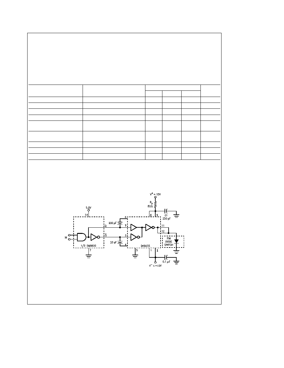
Typical Applications
Grounded Cathode Design
TL K 10124 � 3
Note
Cathode grounded PIN diode R
p
e
62X limits diode forward current to 100 mA Typical switching for
HP33604A RF turn-on 25 ns turn-off 5 ns C2
e
250 pF R
p
e
0X C1
e
0 1F
2
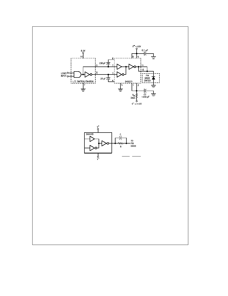
Typical Applications
(Continued)
Grounded Anode Design
TL K 10124 � 4
Note
Anode Grounded PIN diode R
M
e
56X limits diode forward current to 100 mA Typical switching for
HP33622A RF turn-on 5 ns turn-off 4 ns C1
e
470 pF C2
e
0 1 mF R
M
e
0X
Alternate Current Limiting
TL K 10124 � 5
R
e
V
a
b
2
l
f
or
l
V
b
l
b
2
l
f
3
DH0035DH0035C
PIN
Diode
Driver
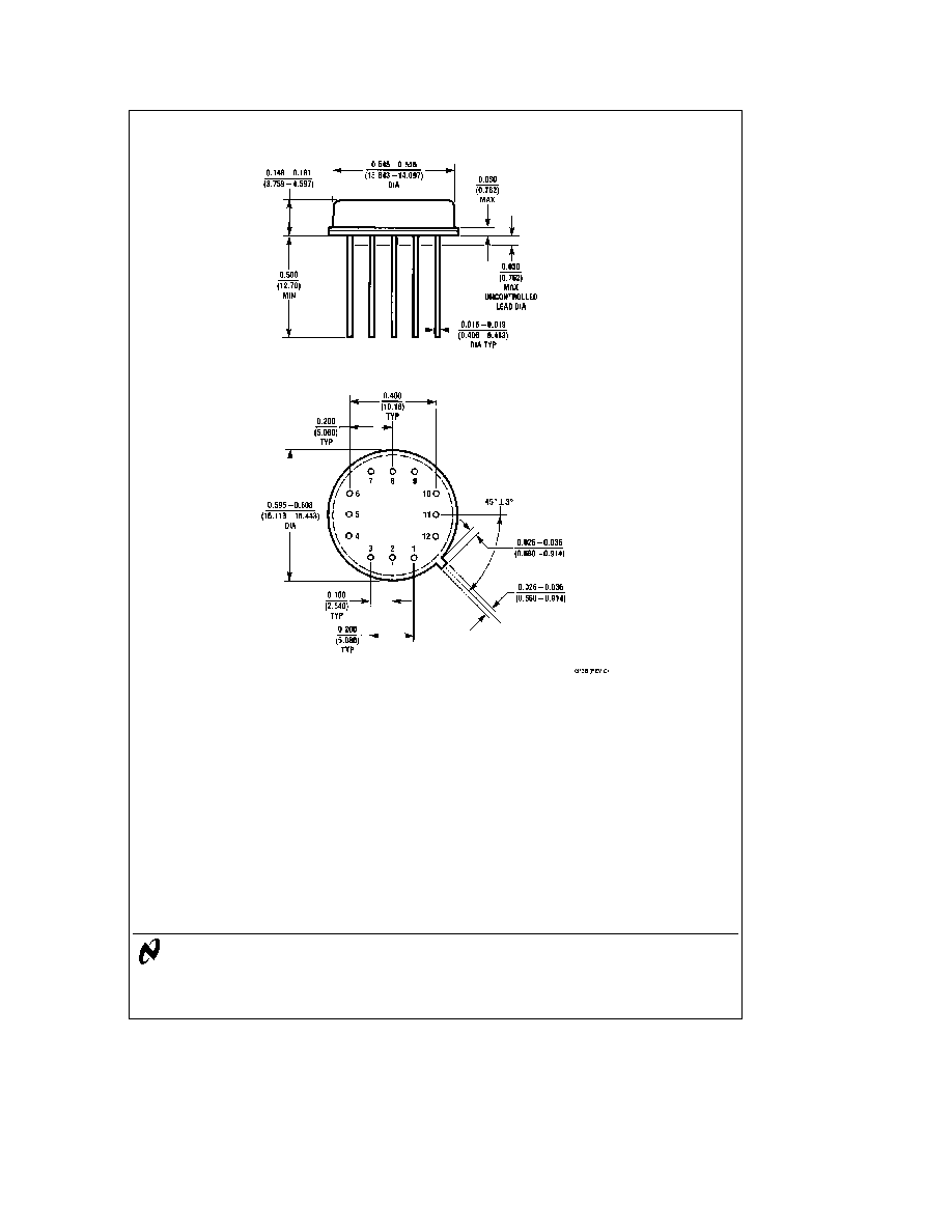
Physical Dimensions
inches (millimeters)
12 Lead Metal Can Package
Order Number DH0035G-MIL or DH0035CG
NS Package Number G12B
LIFE SUPPORT POLICY
NATIONAL'S PRODUCTS ARE NOT AUTHORIZED FOR USE AS CRITICAL COMPONENTS IN LIFE SUPPORT
DEVICES OR SYSTEMS WITHOUT THE EXPRESS WRITTEN APPROVAL OF THE PRESIDENT OF NATIONAL
SEMICONDUCTOR CORPORATION As used herein
1 Life support devices or systems are devices or
2 A critical component is any component of a life
systems which (a) are intended for surgical implant
support device or system whose failure to perform can
into the body or (b) support or sustain life and whose
be reasonably expected to cause the failure of the life
failure to perform when properly used in accordance
support device or system or to affect its safety or
with instructions for use provided in the labeling can
effectiveness
be reasonably expected to result in a significant injury
to the user
National Semiconductor
National Semiconductor
National Semiconductor
National Semiconductor
Corporation
Europe
Hong Kong Ltd
Japan Ltd
1111 West Bardin Road
Fax (a49) 0-180-530 85 86
13th Floor Straight Block
Tel 81-043-299-2309
Arlington TX 76017
Email cnjwge tevm2 nsc com
Ocean Centre 5 Canton Rd
Fax 81-043-299-2408
Tel 1(800) 272-9959
Deutsch Tel (a49) 0-180-530 85 85
Tsimshatsui Kowloon
Fax 1(800) 737-7018
English
Tel (a49) 0-180-532 78 32
Hong Kong
Fran ais Tel (a49) 0-180-532 93 58
Tel (852) 2737-1600
Italiano
Tel (a49) 0-180-534 16 80
Fax (852) 2736-9960
National does not assume any responsibility for use of any circuitry described no circuit patent licenses are implied and National reserves the right at any time without notice to change said circuitry and specifications