 | –≠–ª–µ–∫—Ç—Ä–æ–Ω–Ω—ã–π –∫–æ–º–ø–æ–Ω–µ–Ω—Ç: DM2502J | –°–∫–∞—á–∞—Ç—å:  PDF PDF  ZIP ZIP |
TL F 5702
DM2502
DM2503
DM2504
Successive
Approximation
Registers
November 1995
DM2502 DM2503 DM2504 Successive Approximation
Registers
General Description
The DM2502 DM2503 and DM2504 are 8-bit and 12-bit
TTL registers designed for use in successive approximation
A D converters These devices contain all the logic and
control circuits necessary in combination with a D A con-
verter to perform successive approximation analog-to-digital
conversions
The DM2502 has 8 bits with serial capability and is not ex-
pandable The DM2503 has 8 bits and is expandable with-
out serial capability The DM2504 has 12 bits with serial
capability and expandability
All three devices are available in ceramic DIP ceramic flat-
pak and molded Epoxy-B DIPs The DM2502 DM2503 and
DM2504 operate over
b
55 C to
a
125 C the DM2502C
DM2503C and DM2504C operate over 0 C to
a
70 C
Features
Y
Complete logic for successive approximation A D con-
verters
Y
8-bit and 12-bit registers
Y
Capable of short cycle or expanded operation
Y
Continuous or start-stop operation
Y
Compatible with D A converters using any logic code
Y
Active low or active high logic outputs
Y
Use as general purpose serial-to-parallel converter or
ring counter
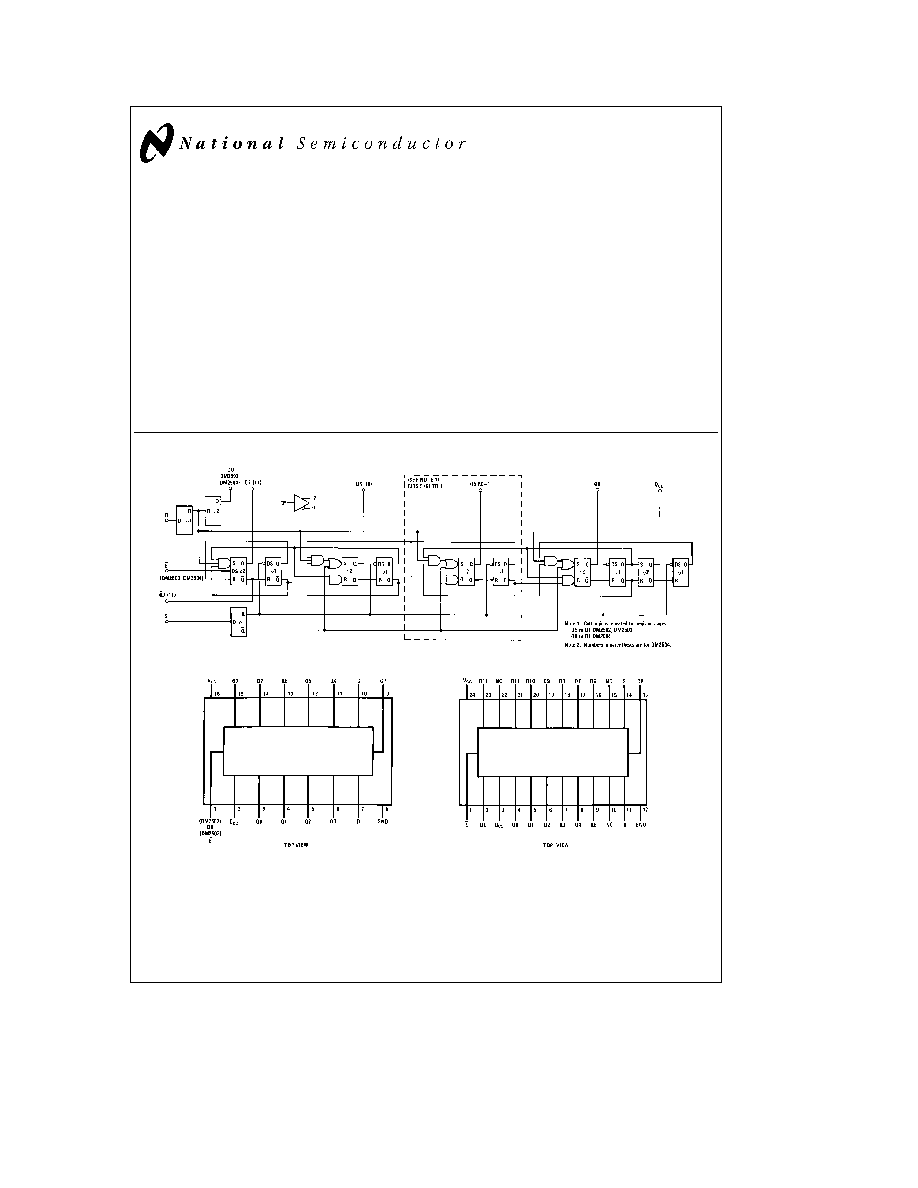
Logic Diagram
Connection Diagrams
(Dual-In-Line and Flat Packages)
DM2502 DM2503
DM2504
TL F 5702 ≠ 1
Order Number DM2502J DM2502CJ DM2503J
or DM2503CJ
See NS Package J16A
Order Number DM2502CN or DM2503CN
See NS Package N16A
Order Number DM2502W DM2502CW DM2503W
or DM2503CW
See NS Package W16A
Order Number DM2504F or DM2504CJ
See NS Package F24D
Order Number DM2504J or DM2504CJ
See NS Package J24A
Order Number DM2504CN
See NS Package N24A
C1995 National Semiconductor Corporation
RRD-B30M115 Printed in U S A
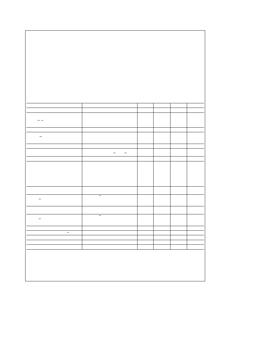
Absolute Maximum Ratings
(Note 1)
Supply Voltage
7V
Input Voltage
5 5V
Output Voltage
5 5V
Storage Temperature Range
b
65 C to
a
150 C
Lead Temperature (Soldering 10 seconds)
300 C
Operating Conditions
Min
Max
Units
Supply Voltage V
CC
DM2502C DM2503C
4 75
5 25
V
DM2504C
DM2502 DM2503
4 5
5 5
V
DM2504
Temperature T
A
DM2502C DM2503C
0
a
70
C
DM2504C
DM2502 DM2503
b
55
a
125
C
DM2504
Electrical Characteristics
(Notes 2 and 3) V
CC
e
5 0V T
A
e
25 C C
L
e
15 pF unless otherwise specified
Parameter
Conditions
Min
Typ
Max
Units
Logical ``1'' Input Voltage (V
IH
)
V
CC
e
Min
2 0
V
Logical ``1'' Input Current (I
IH
)
V
CC
e
Max
CP Input
V
IH
e
2 4V
6
40
m
A
D E S Inputs
V
IH
e
2 4V
6
80
m
A
All Inputs
V
IH
e
5 5V
1 0
mA
Logical ``0'' Input Voltage (V
IL
)
V
CC
e
Min
0 8
V
Logical ``0'' Input Current (I
IL
)
V
CC
e
Max
CP S Inputs
V
IL
e
0 4V
b
1 0
b
1 6
mA
D E Inputs
V
IL
e
0 4V
b
1 0
b
3 2
mA
Logical ``1'' Output Voltage (V
OH
)
V
CC
e
Min I
OH
e
0 48 mA
2 4
3 6
V
Output Short Circuit Current
V
CC
e
Max V
OUT
e
0 0V
b
10
b
20
b
45
mA
(Note 4) (I
OS
)
Output High CP D S High E Low
Logical ``0'' Output Voltage (V
OL
)
V
CC
e
Min I
OL
e
9 6 mA
0 2
0 4
V
Supply Current (I
CC
)
V
CC
e
Max All Outputs Low
DM2502C
65
95
mA
DM2502
65
85
mA
DM2503C
60
90
mA
DM2503
60
80
mA
DM2504C
90
124
mA
DM2504
90
110
mA
Propagation Delay to a Logical ``0''
10
18
28
ns
From CP to Any Output (t
pd0
)
Propagation Delay to a Logical ``0''
CP High S Low
16
24
ns
From E to Q7 (Q11) Output (t
pd0
)
DM2503 DM2503C DM2504
DM2504C Only
Propagation Delay to a Logical ``1''
10
26
38
ns
From CP to Any Output (t
pd1
)
Propagation Delay to a Logical ``1''
CP High S Low
13
19
ns
From E to Q7 (Q11) Output (t
pd1
)
DM2503 DM2503C DM2504
DM2504C Only
Set-Up Time Data Input (t
s(D)
)
b
10
4
8
ns
Set-Up Time Start Input (t
s(S
)
0
9
16
ns
Minimum Low CP Width (t
PWL
)
30
42
ns
Minimum High CP Width (t
PWH
)
17
24
ns
Maximum Clock Frequency (f
MAX
)
15
21
MHz
Note 1
``Absolute Maximum Ratings'' are those values beyond which the safety of the device cannot be guaranteed Except for ``Operating Temperature Range''
they are not meant to imply that the devices should be operated at these limits The table of ``Electrical Characteristics'' provides conditions for actual device
operation
Note 2
Unless otherwise specified min max limits apply across the
b
55 C to
a
125 C temperature range for the DM2502 DM2503 and DM2504 and across the
0 C to
a
70 C range for the DM2502C DM2503C and DM2504C All typicals are given for V
CC
e
5 0V and T
A
e
25 C
Note 3
All currents into device pins shown as positive out of device pins as negative all voltages referenced to ground unless otherwise noted All values shown
as max or min on absolute value basis
Note 4
Only one output at a time should be shorted
2
Application Information
OPERATION
The registers consist of a set of master latches that act as
the control elements in the device and change state on the
input clock high-to-low transition and a set of slave latches
that hold the register data and change on the input clock
low-to-high transition Externally the device acts as a special
purpose serial-to-parallel converter that accepts data at the
D input of the register and sends the data to the appropriate
slave latch to appear at the register output and the DO out-
put on the DM2502 and DM2504 when the clock goes from
low-to-high There are no restrictions on the data input it
can change state at any time except during a short interval
centered about the clock low-to-high transition At the same
time that data enters the register bit the next less significant
bit register is set to a low ready for the next iteration
The register is reset by holding the S (Start) signal low dur-
ing the clock low-to-high transition The register synchro-
nously resets to the state Q7 (11) low and all the remaining
register outputs high The Q
CC
(Conversion Complete) sig-
nal is also set high at this time The S signal should not be
brought back high until after the clock low-to-high transition
in order to guarantee correct resetting After the clock has
gone high resetting the register the S signal must be re-
moved On the next clock low-to-high transition the data on
the D input is set into the Q7 (11) register bit and the Q6
(10) register bit is set to a low ready for the next clock cycle
On the next clock low-to-high transition data enters the Q6
(10) register bit and Q5 (9) is set to a low This operation is
repeated for each register bit in turn until the register has
been filled When the data goes into Q0 the Q
CC
signal
goes low and the register is inhibited from further change
until reset by a Start signal
The DM2502 DM2503 and DM2504 have a specially tai-
lored two-phase clock generator to provide nonoverlapping
two-phase clock pulses (i e the clock waveforms intersect
below the thresholds of the gates they drive) Thus even at
very slow dV dt rates at the clock input (such as from rela-
tively weak comparator outputs) improper logic operation
will not result
LOGIC CODES
All three registers can be operated with various logic codes
Two's complement code is used by offsetting the compara-
tor
full range
a
LSB and using the complement of the
MSB (Q7 or Q11) with a binary D A converter Offset binary
is used in the same manner but with the MSB (Q7 or Q11)
BCD D A converters can be used with the addition of illegal
code suppression logic
ACTIVE HIGH OR ACTIVE LOW LOGIC
The register can be used with either D A converters that
require a low voltage level to turn on or D A converters that
require a high voltage level to turn the switch on If D A
converters are used which turn on with a low logic level the
resulting digital output from the register is active low That
is a logic ``1'' is represented as a low voltage level If D A
converters are used that turn on with a high logic level then
the digital output is active high a logic ``1'' is represented as
a high voltage level
EXPANDED OPERATION
An active low enable input E on the DM2503 and DM2504
allows registers to be connected together to form a longer
register by connecting the clock D and S inputs in parallel
and connecting the Q
CC
output of one register to the E input
of the next less significant register When the start resets
the register the E signal goes high forcing the Q7 (11) bit
high and inhibiting the register from accepting data until the
previous register is full and its Q
CC
goes low If only one
register is used the E input should be held at a low logic
level
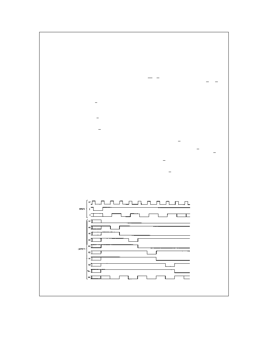
Timing Diagram
DM2502 DM2503
TL F 5702 ≠ 2
3

Application Information
(Continued)
SHORT CYCLE
If all bits are not required the register may be truncated and
conversion time saved by using a register output going low
rather then the Q
CC
signal to indicate the end of conversion
If the register is truncated and operated in the continuous
conversion mode a lock-up condition may occur on power
turn-on This condition can be avoided by making the start
input the OR function of Q
CC
and the appropriate register
output
COMPARATOR BIAS
To minimize the digital error below
g
LSB the compara-
tor must be biased If a D A converter is used which re-
quires a low voltage level to turn on the comparator should
be biased
a
LSB If the D A converter requires a high
logic level to turn on the comparator must be biased
b
LSB
Definition of Terms
CP
The clock input of the register
D
The serial data input of the register
DO
The serial data out (The D input delayed one bit)
E
The register enable This input is used to expand the
length of the register and when high forces the Q7 (11)
register output high and inhibits conversion When not used
for expansion the enable is held at a low logic level
(ground)
Q
i
i
e
7 (11) to 0
The outputs of the register
Q
CC
The conversion complete output This output remains
high during a conversion and goes low when a conversion is
complete
Q7 (11)
The true output of the MSB of the register
Q7 (11)
The complement output of the MSB of the register
S
The start input If the start input is held low for at least a
clock period the register will be reset to Q7 (11) low and all
the remaining outputs high A start pulse that is low for a
shorter period of time can be used if it meets the set-up time
requirements of the S input
Truth Table
DM2502 DM2503
Time
Inputs
Outputs
1
t
n
D
S
E
2
D0
3
Q7
Q6
Q5
Q4
Q3
Q2
Q1
Q0
Q
CC
0
X
L
L
X
X
X
X
X
X
X
X
X
X
1
D7
H
L
X
L
H
H
H
H
H
H
H
H
2
D6
H
L
D7
D7
L
H
H
H
H
H
H
H
3
D5
H
L
D6
D7
D6
L
H
H
H
H
H
H
4
D4
H
L
D5
D7
D6
D5
L
H
H
H
H
H
5
D3
H
L
D4
D7
D6
D5
D4
L
H
H
H
H
6
D2
H
L
D3
D7
D6
D5
D4
D3
L
H
H
H
7
D1
H
L
D2
D7
D6
D5
D4
D3
D2
L
H
H
8
D0
H
L
D1
D7
D6
D5
D4
D3
D2
D1
L
H
9
X
H
L
D0
D7
D6
D5
D4
D3
D2
D1
D0
L
10
X
X
L
X
D7
D6
D5
D4
D3
D2
D1
D0
L
X
X
H
X
H
NC
NC
NC
NC
NC
NC
NC
NC
H
e
High Voltage Level
Note 1
Truth table for DM2504 is extended to include 12 outputs
L
e
Low Voltage Level
Note 2
Truth table for DM2502 does not include E column or last line in truth table shown
X
e
Don't Care
Note 3
Truth table for DM2503 does not include D0 column
NC
e
No Change
Typical Applications
BCD Illegal Code Suppression
Active High
Active Low
TL F 5702 ≠ 3
4
Typical Applications
(Continued)
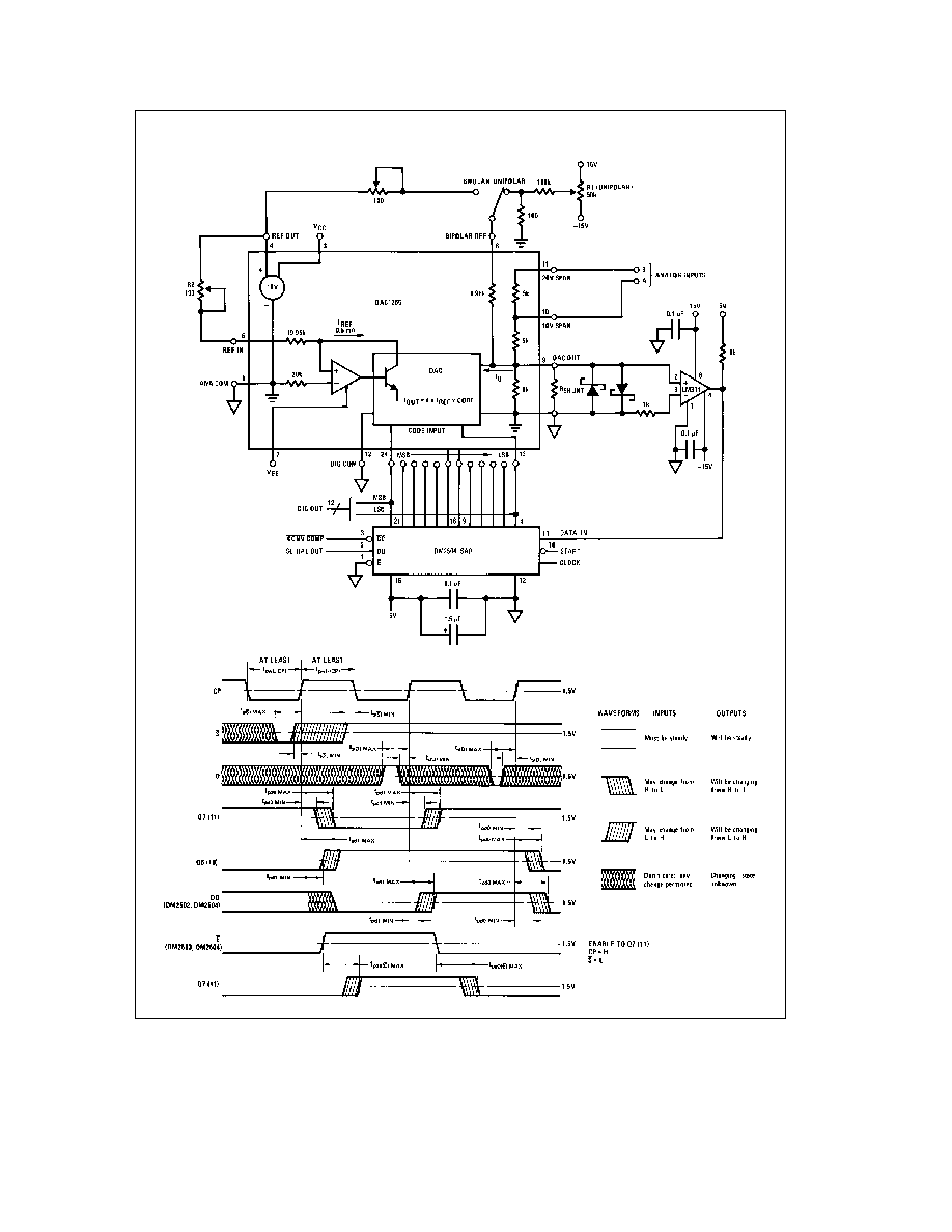
Fast Precision Analog-to-Digital Converter
INPUT RANGES
Equiv
Unipolar
Bipolar
Connect
DAC Z
OUT
0 to 10
g
5
Input to A
2 36 kX
0 to 5
g
2 5
Input to A
1 90 kX
0 to 20
g
10
Input to B
3 08 kX
B to DAC OUT
Switching Time Waveforms
TL F 5702 ≠ 4
TL F 5702 ≠ 5
5