 | –≠–ª–µ–∫—Ç—Ä–æ–Ω–Ω—ã–π –∫–æ–º–ø–æ–Ω–µ–Ω—Ç: DM54L72J | –°–∫–∞—á–∞—Ç—å:  PDF PDF  ZIP ZIP |
TL F 6629
DM54L72
AND-Gated
Master-Slave
J-K
Flip-Flop
with
Preset
Clear
and
Complementary
Outputs
June 1989
DM54L72 AND-Gated Master-Slave J-K Flip-Flop
with Preset Clear and Complementary Outputs
General Description
This device contains a positive pulse triggered master-slave
J-K flip-flop with complementary outputs Multiple J and K
inputs are ANDed together to produce the internal J and K
function for the flip-flop The J and K data is processed by
the flip-flop after a complete clock pulse While the clock is
low the slave is isolated from the master On the positive
transition of the clock the data from the AND gates is trans-
ferred to the master While the clock is high the AND gate
inputs are disabled On the negative transition of the clock
the data from the master is transferred to the slave The
logic state of the J and K inputs must not be allowed to
change while the clock is in the high state Data is trans-
ferred to the outputs on the falling edge of the clock pulse
A low logic level on the preset or clear inputs sets or resets
the outputs regardless of the logic levels of the other inputs
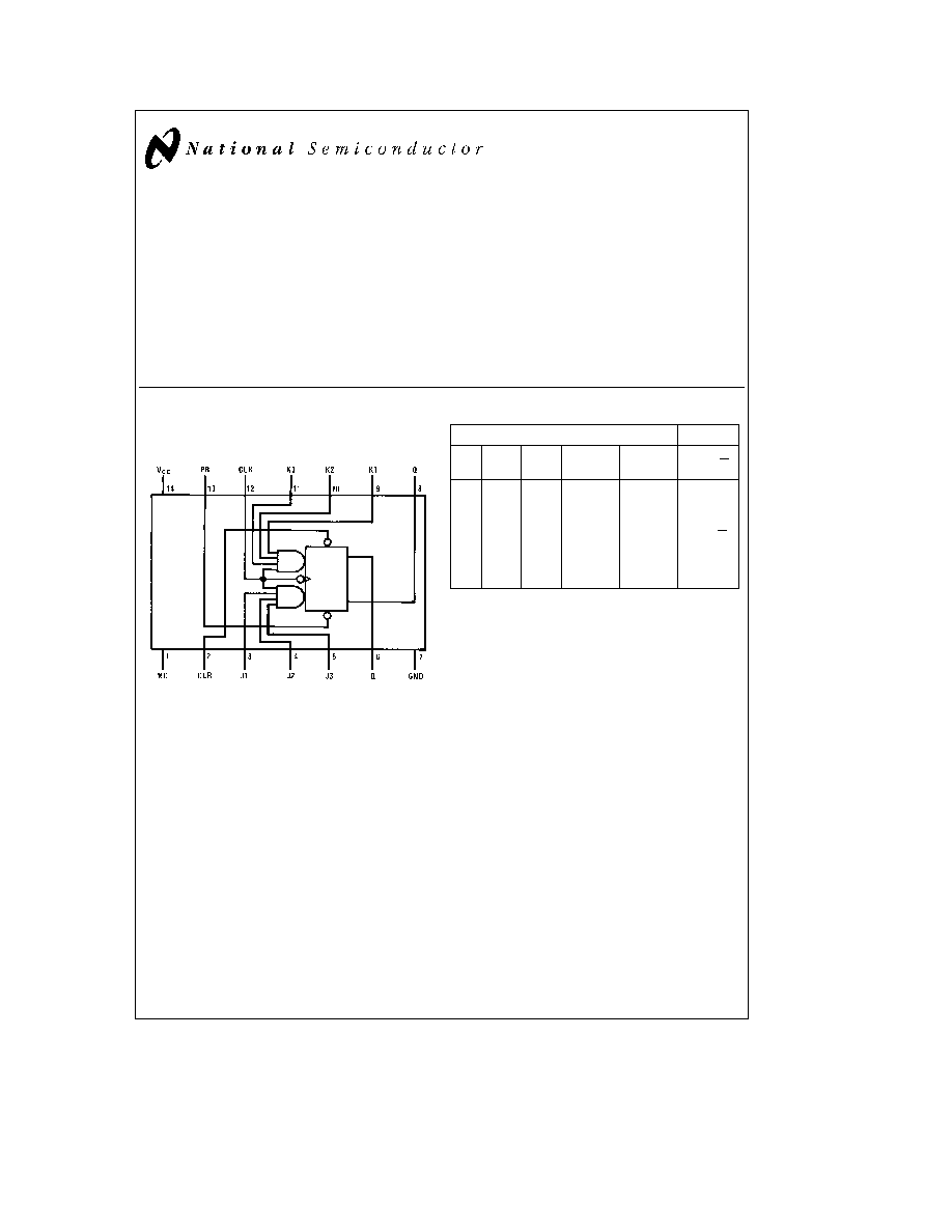
Connection Diagram
Dual-In-Line Package
TL F 6629 ≠ 1
Order Number DM54L72J or DM54L72W
See NS Package Number J14A or W14B
Function Table
Inputs
Outputs
PR
CLR
CLK
J
K
Q
Q
(Note 1)
(Note 1)
L
H
X
X
X
H
L
H
L
X
X
X
L
H
L
L
X
X
X
H
H
H
H
L
L
Q
o
Q
o
H
H
H
L
H
L
H
H
L
H
L
H
H
H
H
H
Toggle
Note 1
J
e
(J1)(J2)(J3) K
e
(K1)(K2)(K3)
H
e
High Logic Level
X
e
Either Low or High Logic Level
L
e
Low Logic Level
e
Positive pulse The J and K inputs must be held constant while the
clock is high Data is transferred to the outputs on the falling edge of the
clock pulse
Q
o
e
The output logic level before the indicated input conditions were es-
tablished
e
This configuration is nonstable that is it will not persist when the preset
and or clear inputs return to their inactive (high) level
Toggle
e
Each output changes to the complement of its previous level on
each complete high level clock pulse
C1995 National Semiconductor Corporation
RRD-B30M105 Printed in U S A
Absolute Maximum Ratings
(Note)
If Military Aerospace specified devices are required
please contact the National Semiconductor Sales
Office Distributors for availability and specifications
Supply Voltage
8V
Input Voltage
5 5V
Operating Free Air Temperature Range
DM54L
b
55 C to
a
125 C
Storage Temperature Range
b
65 C to
a
150 C
Note
The ``Absolute Maximum Ratings'' are those values
beyond which the safety of the device cannot be guarateed
The device should not be operated at these limits The para-
metric values defined in the ``Electrical Characteristics'' ta-
ble are not guaranteed at the absolute maximum ratings
The ``Recommended Operating Conditions'' table will define
the conditions for actual device operation
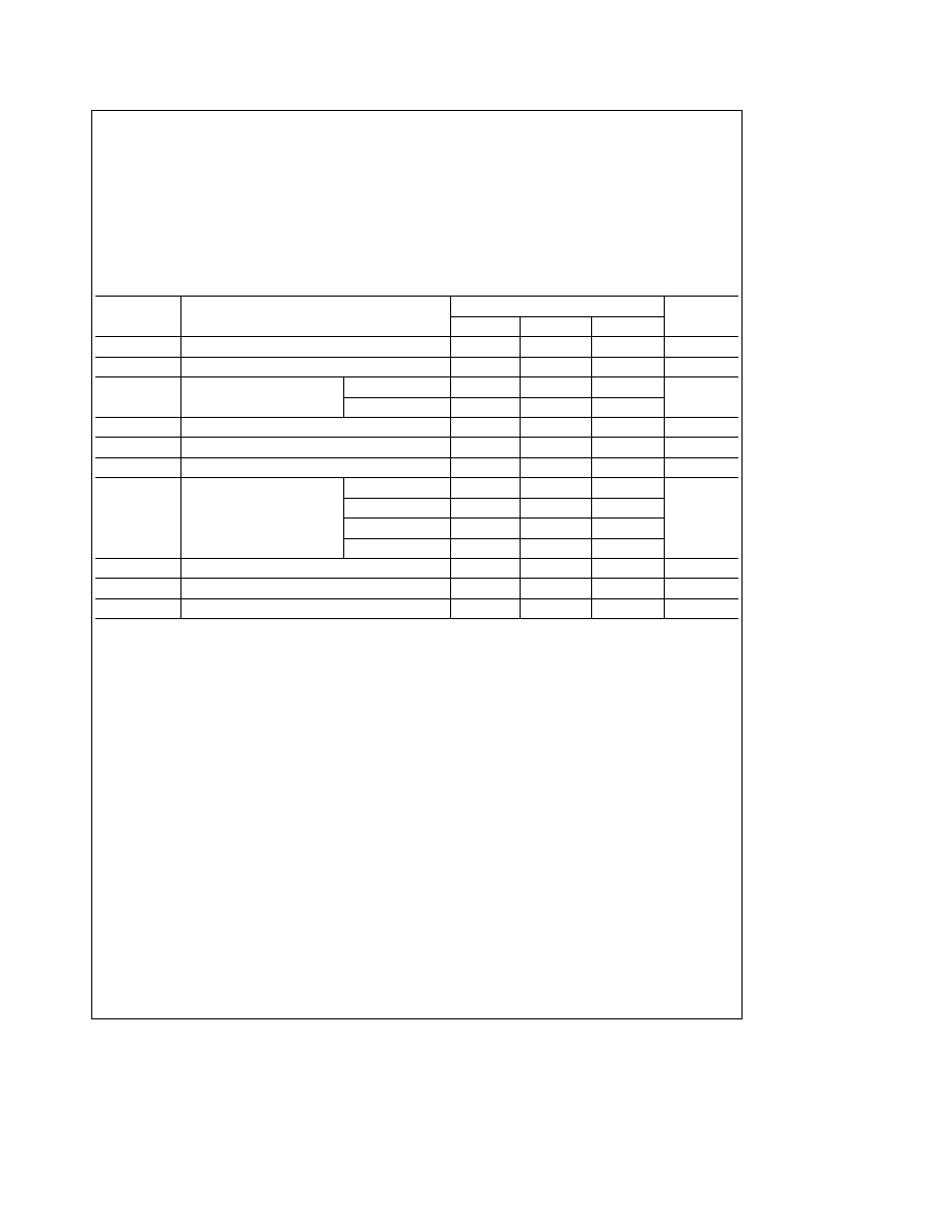
Recommended Operating Conditions
Symbol
Parameter
DM54L72
Units
Min
Nom
Max
V
CC
Supply Voltage
4 5
5
5 5
V
V
IH
High Level Input Voltage
2
V
V
IL
Low Level Input Voltage
Clock
0 6
V
Others
0 7
I
OH
High Level Output Current
b
0 2
mA
I
OL
Low Level Output Current
2
mA
f
CLK
Clock Frequency (Note 2)
0
6
MHz
t
W
Pulse Width (Note 2)
Clock High
100
Clock Low
100
ns
Preset Low
100
Clear Low
100
t
SU
Input Setup Time (Notes 1
2)
0
u
ns
t
H
Input Hold Time (Notes 1
2)
0
v
ns
T
A
Free Air Operating Temperature
b
55
125
C
Note 1
The symbols (
u v
) indicate the edge of the clock pulse used for reference
u
for rising edge
v
for falling edge
Note 2
T
A
e
25 C and V
CC
e
5V
2
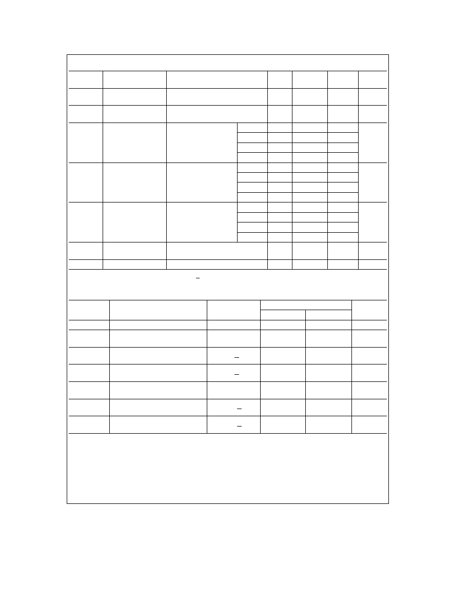
Electrical Characteristics
over recommended operating free air temperature (unless otherwise noted)
Symbol
Parameter
Conditions
Min
Typ
Max
Units
(Note 1)
V
OH
High Level Output
V
CC
e
Min I
OH
e
Max
2 4
3 3
V
Voltage
V
IL
e
Max V
IH
e
Min
V
OL
Low Level Output
V
CC
e
Min I
OL
e
Max
0 15
0 3
V
Voltage
V
IL
e
Max V
IH
e
Min
I
I
Input Current
Max
V
CC
e
Max
J K
100
Input Voltage
V
I
e
5 5V
Clear
200
m
A
Preset
200
Clock
200
I
IH
High Level Input
V
CC
e
Max
J K
10
Current
V
I
e
2 4V
Clear
20
m
A
Preset
20
Clock
b
200
I
IL
Low Level Input
V
CC
e
Max
J K
b
0 18
Current
V
I
e
0 3V
Clear
b
0 36
mA
Preset
b
0 36
Clock
b
0 36
I
OS
Short Circuit
V
CC
e
Max
b
3
b
15
mA
Output Current
I
CC
Supply Current
V
CC
e
Max (Note 2)
0 76
1 44
mA
Note 1
All typicals are at V
CC
e
5V T
A
e
25 C
Note 2
With all outputs open I
CC
is measured with the Q and Q outputs high in turn At the time of measurement the clock input is grounded
Switching Characteristics
at V
CC
e
5V and T
A
e
25 C (See Section 1 for Test Waveforms and Output Load)
Symbol
Parameter
From (Input)
R
L
e
4 kX C
L
e
50 pF
Units
To (Output)
Min
Max
f
MAX
Maximum Clock Frequency
6
MHz
t
PLH
Propagation Delay Time
Preset
75
ns
Low to High Level Output
to Q
t
PHL
Propagation Delay Time
Preset
150
ns
High to Low Level Output
to Q
t
PLH
Propagation Delay Level Output
Clear
75
ns
Low to High Level Output
to Q
t
PHL
Propagation Delay Time
Clear
150
ns
High to Low Level Output
to Q
t
PLH
Propagation Delay Time
Clock to
10
75
ns
Low to High Level Output
Q or Q
t
PHL
Propagation Delay Time
Clock to
10
150
ns
High to Low Level Output
Q or Q
3
DM54L72
AND-Gated
Master-Slave
J-K
Flip-Flop
with
Preset
Clear
and
Complementary
Outputs
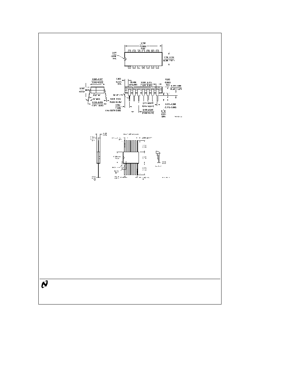
Physical Dimensions
inches (millimeters)
14-Lead Ceramic Dual-In-Line Package (J)
Order Number DM54L72J
NS Package Number J14A
14-Lead Ceramic Flat Package (W)
Order Number DM54L72W
NS Package Number W14B
LIFE SUPPORT POLICY
NATIONAL'S PRODUCTS ARE NOT AUTHORIZED FOR USE AS CRITICAL COMPONENTS IN LIFE SUPPORT
DEVICES OR SYSTEMS WITHOUT THE EXPRESS WRITTEN APPROVAL OF THE PRESIDENT OF NATIONAL
SEMICONDUCTOR CORPORATION As used herein
1 Life support devices or systems are devices or
2 A critical component is any component of a life
systems which (a) are intended for surgical implant
support device or system whose failure to perform can
into the body or (b) support or sustain life and whose
be reasonably expected to cause the failure of the life
failure to perform when properly used in accordance
support device or system or to affect its safety or
with instructions for use provided in the labeling can
effectiveness
be reasonably expected to result in a significant injury
to the user
National Semiconductor
National Semiconductor
National Semiconductor
National Semiconductor
Corporation
Europe
Hong Kong Ltd
Japan Ltd
1111 West Bardin Road
Fax (a49) 0-180-530 85 86
13th Floor Straight Block
Tel 81-043-299-2309
Arlington TX 76017
Email cnjwge tevm2 nsc com
Ocean Centre 5 Canton Rd
Fax 81-043-299-2408
Tel 1(800) 272-9959
Deutsch Tel (a49) 0-180-530 85 85
Tsimshatsui Kowloon
Fax 1(800) 737-7018
English
Tel (a49) 0-180-532 78 32
Hong Kong
Fran ais Tel (a49) 0-180-532 93 58
Tel (852) 2737-1600
Italiano
Tel (a49) 0-180-534 16 80
Fax (852) 2736-9960
National does not assume any responsibility for use of any circuitry described no circuit patent licenses are implied and National reserves the right at any time without notice to change said circuitry and specifications