
TL F 6392
54LS151DM54LS151DM74LS151
Data
SelectorMultiplexer
June 1989
54LS151 DM54LS151 DM74LS151
Data Selector Multiplexer
General Description
This data selector multiplexer contains full on-chip decod-
ing to select the desired data source The 'LS151 selects
one-of-eight data sources The 'LS151 has a strobe input
which must be at a low logic level to enable these devices
A high level at the strobe forces the W output high and the
Y output low
The 'LS151 features complementary W and Y outputs
Features
Y
Select one-of-eight data lines
Y
Performs parallel-to-serial conversion
Y
Permits multiplexing from N lines to one line
Y
Also for use as Boolean function generator
Y
Typical average propagation delay time data input to W
output 12 5 ns
Y
Typical power dissipation 30 mW
Y
Alternate Military Aerospace device (54LS151) is avail-
able Contact a National Semiconductor Sales Office
Distributor for specifications
Connection Diagram
Dual-In-Line Package
TL F 6392 ≠ 1
Order Number 54LS151DMQB 54LS151FMQB 54LS151LMQB
DM54LS151J DM54LS151W DM74LS151M or DM74LS151N
See NS Package Number E20A J16A M16A N16E or W16A
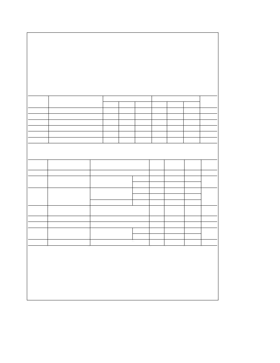
Truth Table
Inputs
Outputs
Select
Strobe
Y
W
C
B
A
S
X
X
X
H
L
H
L
L
L
L
D0
D0
L
L
H
L
D1
D1
L
H
L
L
D2
D2
L
H
H
L
D3
D3
H
L
L
L
D4
D4
H
L
H
L
D5
D5
H
H
L
L
D6
D6
H
H
H
L
D7
D7
H
e
High Level L
e
Low Level X
e
Don't Care
D0 D1 D7
e
the level of the respective D input
C1995 National Semiconductor Corporation
RRD-B30M105 Printed in U S A
Absolute Maximum Ratings
(Note)
If Military Aerospace specified devices are required
please contact the National Semiconductor Sales
Office Distributors for availability and specifications
Supply Voltage
7V
Input Voltage
7V
Operating Free Air Temperature Range
DM54LS and 54LS
b
55 C to
a
125 C
DM74LS
0 C to
a
70 C
Storage Temperature Range
b
65 C to
a
150 C
Note
The ``Absolute Maximum Ratings'' are those values
beyond which the safety of the device cannot be guaran-
teed The device should not be operated at these limits The
parametric values defined in the ``Electrical Characteristics''
table are not guaranteed at the absolute maximum ratings
The ``Recommended Operating Conditions'' table will define
the conditions for actual device operation
Recommended Operating Conditions
Symbol
Parameter
DM54LS151
DM74LS151
Units
Min
Nom
Max
Min
Nom
Max
V
CC
Supply Voltage
4 5
5
5 5
4 75
5
5 25
V
V
IH
High Level Input Voltage
2
2
V
V
IL
Low Level Input Voltage
0 7
0 8
V
I
OH
High Level Output Current
b
0 4
b
0 4
mA
I
OL
Low Level Output Current
4
8
mA
T
A
Free Air Operating Temperature
b
55
125
0
70
C
Electrical Characteristics
over recommended operating free air temperature range (unless otherwise noted)
Symbol
Parameter
Conditions
Min
Typ
Max
Units
(Note 1)
V
I
Input Clamp Voltage
V
CC
e
Min I
I
e b
18 mA
b
1 5
V
V
OH
High Level Output
V
CC
e
Min I
OH
e
Max
DM54
2 5
3 4
V
Voltage
V
IL
e
Max V
IH
e
Min
DM74
2 7
3 4
V
OL
Low Level Output
V
CC
e
Min I
OL
e
Max
DM54
0 25
0 4
Voltage
V
IL
e
Max V
IH
e
Min
DM74
0 35
0 5
V
I
OL
e
4 mA V
CC
e
Min
DM74
0 25
0 4
I
I
Input Current
Max
V
CC
e
Max V
I
e
7V
0 1
mA
Input Voltage
I
IH
High Level Input Current
V
CC
e
Max V
I
e
2 7V
20
m
A
I
IL
Low Level Input Current
V
CC
e
Max V
I
e
0 4V
b
0 4
mA
I
OS
Short Circuit
V
CC
e
Max
DM54
b
20
b
100
mA
Output Current
(Note 2)
DM74
b
20
b
100
I
CC
Supply Current
V
CC
e
Max (Note 3)
6
10
mA
Note 1
All typicals are at V
CC
e
5V T
A
e
25 C
Note 2
Not more than one output should be shorted at a time and the duration should not exceed one second
Note 3
I
CC
is measured with all outputs open strobe and data select inputs at 4 5V and all other inputs open
2
Switching Characteristics
at V
CC
e
5V and T
A
e
25 C (See Section 1 for Test Waveforms and Output Load)
From (Input)
R
L
e
2 kX
Symbol
Parameter
To (output)
C
L
e
15 pF
C
L
e
50 pF
Units
Min
Max
Min
Max
t
PLH
Propagation Delay Time
Select
43
46
ns
Low to High Level Output
(4 Levels) to Y
t
PHL
Propagation Delay Time
Select
30
36
ns
High to Low Level Output
(4 Levels) to Y
t
PLH
Propagation Delay Time
Select
23
25
ns
Low to High Level Output
(3 Levels) to W
t
PHL
Propagation Delay Time
Select
32
40
ns
High to Low Level Output
(3 Levels) to W
t
PLH
Propagation Delay Time
Strobe
42
44
ns
Low to High Level Output
to Y
t
PHL
Propagation Delay Time
Strobe
32
40
ns
High to Low Level Output
to Y
t
PLH
Propagation Delay Time
Strobe
24
27
ns
Low to High Level Output
to W
t
PHL
Propagation Delay Time
Strobe
30
36
ns
High to Low Level Output
to W
t
PLH
Propagation Delay Time
D0 thru D7
32
35
ns
Low to High Level Output
to Y
t
PHL
Propagation Delay Time
D0 thru D7
26
33
ns
High to Low Level Output
to Y
t
PLH
Propagation Delay Time
D0 thru D7
21
25
ns
Low to High Level Output
to W
t
PHL
Propagation Delay Time
D0 thru D7
20
27
ns
High to Low Level Output
to W
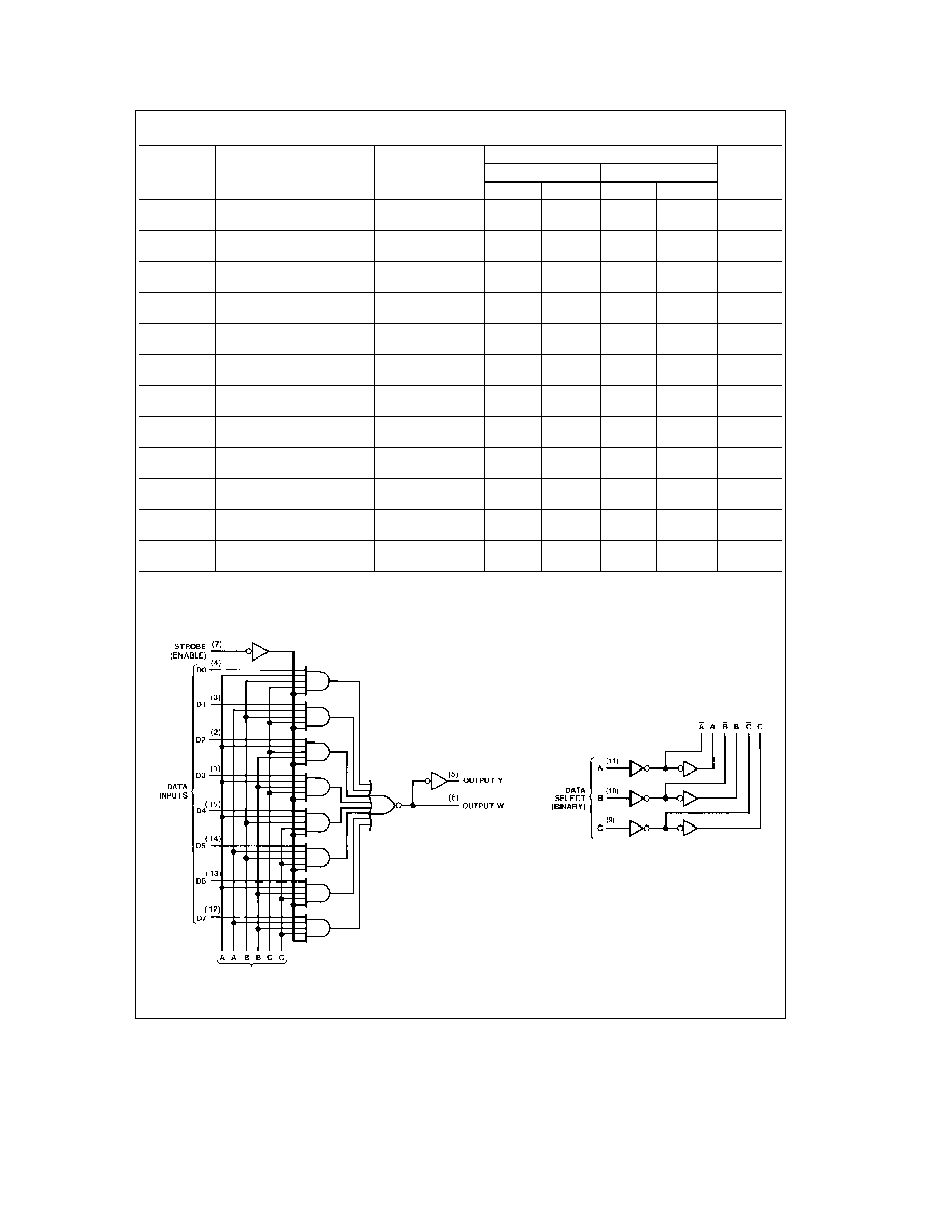
Logic Diagram
LS151
TL F 6392 ≠ 2
See Address Buffers to the Right
Address Buffers for 54LS151 74LS151
TL F 6392 ≠ 3
3
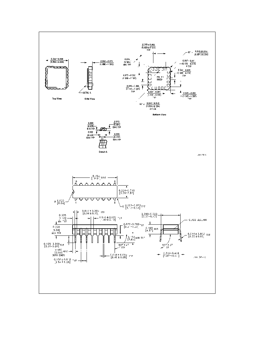
Physical Dimensions
inches (millimeters)
Ceramic Leadless Chip Carrier Package (E)
Order Number 54LS151LMQB
NS Package Number E20A
Ceramic Dual-In-Line Package (J)
Order Number 54LS151DMQB or DM54LS151J
NS Package Number J16A
4

Physical Dimensions
inches (millimeters) (Continued)
16-Lead Small Outline Molded Package (M)
Order Number DM74LS151M
NS Package Number M16A
16-Lead Molded Dual-In-Line Package (N)
Order Number DM74LS151N
NS Package Number N16E
5