TL F 6404
54LS174DM54LS174DM74LS174
54LS175DM54LS175DM74LS175
HexQuad
D
Flip-Flops
with
Clear
June 1989
54LS174 DM54LS174 DM74LS174
54LS175 DM54LS175 DM74LS175
Hex Quad D Flip-Flops with Clear
General Description
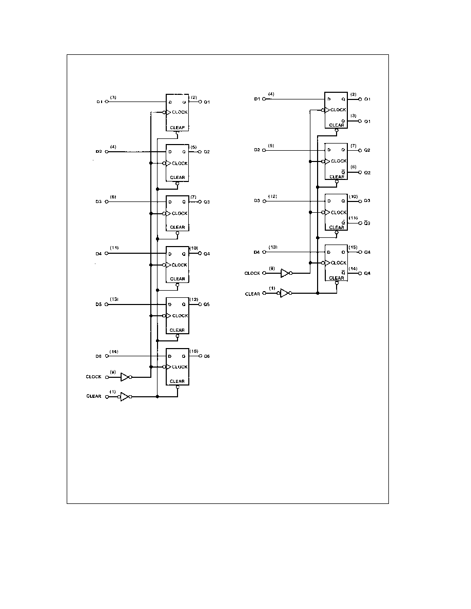
These positive-edge-triggered flip-flops utilize TTL circuitry
to implement D-type flip-flop logic All have a direct clear
input and the quad (175) versions feature complementary
outputs from each flip-flop
Information at the D inputs meeting the setup time require-
ments is transferred to the Q outputs on the positive-going
edge of the clock pulse Clock triggering occurs at a particu-
lar voltage level and is not directly related to the transition
time of the positive-going pulse When the clock input is at
either the high or low level the D input signal has no effect
at the output
Features
Y
LS174 contains six flip-flops with single-rail outputs
Y
LS175 contains four flip-flops with double-rail outputs
Y
Buffered clock and direct clear inputs
Y
Individual data input to each flip-flop
Y
Applications include
Buffer storage registers
Shift registers
Pattern generators
Y
Typical clock frequency 40 MHz
Y
Typical power dissipation per flip-flop 14 mW
Y
Alternate
Military Aerospace
device
(54LS174
54LS175) is available Contact a National Semiconduc-
tor Sales Office Distributor for specifications
Connection Diagrams
Dual-In-Line Package
TL F 6404 ≠ 1
Order Number 54LS174DMQB 54LS174FMQB
54LS174LMQB DM54LS174J
DM54LS174W DM74LS174M or DM74LS174N
See NS Package Number E20A J16A
M16A N16E or W16A
Dual-In-Line Package
TL F 6404 ≠ 2
Order Number 54LS175DMQB 54LS175FMQB
54LS175LMQB DM54LS175J
DM54LS175W DM74LS175M or DM74LS175N
See NS Package Number E20A J16A
M16A N16E or W16A
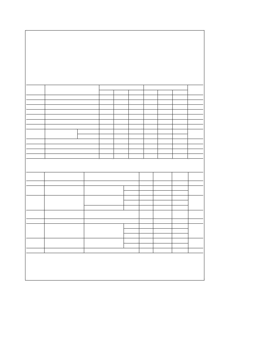
Function Table
(Each Flip-Flop)
Inputs
Outputs
Clear
Clock
D
Q
Q
L
X
X
L
H
H
u
H
H
L
H
u
L
L
H
H
L
X
Q
0
Q
0
H
e
High Level (steady state)
L
e
Low Level (steady state)
X
e
Don't Care
u
e
Transition from low to high level
Q
0
e
The level of Q before the indicated steady-state input conditions were
established
e
LS175 only
C1995 National Semiconductor Corporation
RRD-B30M105 Printed in U S A
Absolute Maximum Ratings
(Note)
If Military Aerospace specified devices are required
please contact the National Semiconductor Sales
Office Distributors for availability and specifications
Supply Voltage
7V
Input Voltage
7V
Operating Free Air Temperature Range
DM54LS and 54LS
b
55 C to
a
125 C
DM74LS
0 C to
a
70 C
Storage Temperature Range
b
65 C to
a
150 C
Note
The ``Absolute Maximum Ratings'' are those values
beyond which the safety of the device cannot be guaran-
teed The device should not be operated at these limits The
parametric values defined in the ``Electrical Characteristics''
table are not guaranteed at the absolute maximum ratings
The ``Recommended Operating Conditions'' table will define
the conditions for actual device operation
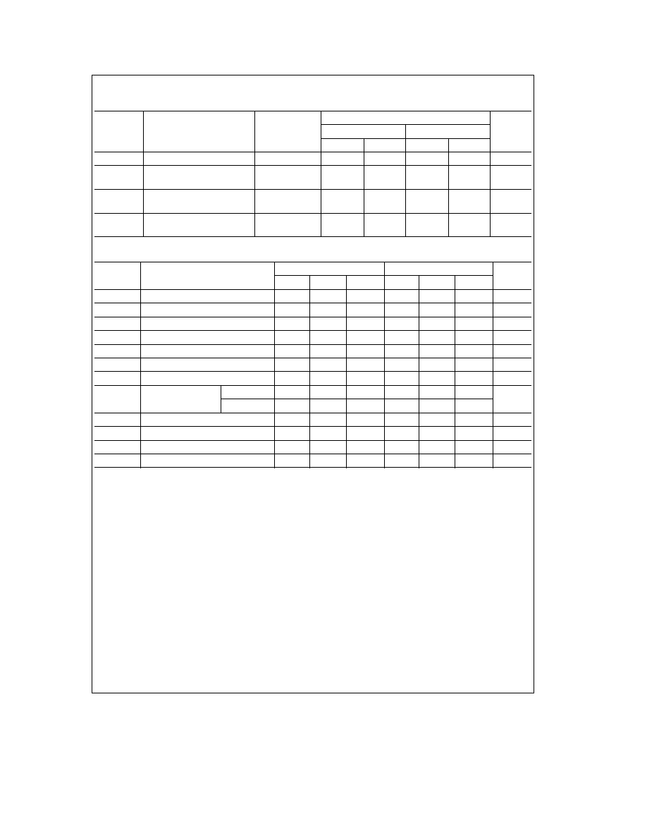
Recommended Operating Conditions
Symbol
Parameter
DM54LS174
DM74LS174
Units
Min
Nom
Max
Min
Nom
Max
V
CC
Supply Voltage
4 5
5
5 5
4 75
5
5 25
V
V
IH
High Level Input Voltage
2
2
V
V
IL
Low Level Input Voltage
0 7
0 8
V
I
OH
High Level Output Current
b
0 4
b
0 4
mA
I
OL
Low Level Output Current
4
8
mA
f
CLK
Clock Frequency (Note 1)
0
30
0
30
MHz
f
CLK
Clock Frequency (Note 2)
0
25
0
25
MHz
t
W
Pulse Width
Clock
20
20
ns
(Note 6)
Clear
20
20
t
SU
Data Setup Time (Note 6)
20
20
ns
t
H
Data Hold Time (Note 6)
0
0
ns
t
REL
Clear Release Time (Note 6)
25
25
ns
T
A
Free Air Operating Temperature
b
55
125
0
70
C
'LS174 Electrical Characteristics
over recommended operating free air temperature range (unless otherwise noted)
Symbol
Parameter
Conditions
Min
Typ
Max
Units
(Note 3)
V
I
Input Clamp Voltage
V
CC
e
Min I
I
e b
18 mA
b
1 5
V
V
OH
High Level Output
V
CC
e
Min I
OH
e
Max
DM54
2 5
3 4
V
Voltage
V
IL
e
Max V
IH
e
Min
DM74
2 7
3 4
V
OL
Low Level Output
V
CC
e
Min I
OL
e
Max
DM54
0 25
0 4
Voltage
V
IL
e
Max V
IH
e
Min
DM74
0 35
0 5
V
I
OL
e
4 mA V
CC
e
Min
DM74
0 25
0 4
I
I
Input Current Max
V
CC
e
Max V
I
e
7V
0 1
mA
Input Voltage
I
IH
High Level Input Current
V
CC
e
Max V
I
e
2 7V
20
m
A
I
IL
Low Level Input
V
CC
e
Max
Clock
b
0 4
Current
V
I
e
0 4V
Clear
b
0 4
mA
Data
b
0 36
I
OS
Short Circuit
V
CC
e
Max
DM54
b
20
b
100
mA
Output Current
(Note 4)
DM74
b
20
b
100
I
CC
Supply Current
V
CC
e
Max (Note 5)
16
26
mA
Note 1
C
L
e
15 pF R
L
e
2 kX T
A
e
25 C and V
CC
e
5V
Note 2
C
L
e
50 pF R
L
e
2 kX T
A
e
25 C and V
CC
e
5V
Note 3
All typicals are at V
CC
e
5V T
A
e
25 C
Note 4
Not more than one output should be shorted at a time and the duration should not exceed one second
Note 5
With all outputs open and 4 5V applied to all data and clear inputs I
CC
is measured after a momentary ground then 4 5V applied to the clock
Note 6
T
A
e
25 C and V
CC
e
5V
2
'LS174 Switching Characteristics
at V
CC
e
5V and T
A
e
25 C (See Section 1 for Test Waveforms and Output Load)
From (Input)
R
L
e
2 kX
Symbol
Parameter
To (Output)
C
L
e
15 pF
C
L
e
50 pF
Units
Min
Max
Min
Max
f
MAX
Maximum Clock Frequency
30
25
MHz
t
PLH
Propagation Delay Time
Clock to
30
32
ns
Low to High Level Output
Output
t
PHL
Propagation Delay Time
Clock to
30
36
ns
High to Low Level Output
Output
t
PHL
Propagation Delay Time
Clear to
35
42
ns
High to Low Level Output
Output
Recommended Operating Conditions
Symbol
Parameter
DM54LS175
DM74LS175
Units
Min
Nom
Max
Min
Nom
Max
V
CC
Supply Voltage
4 5
5
5 5
4 75
5
5 25
V
V
IH
High Level Input Voltage
2
2
V
V
IL
Low Level Input Voltage
0 7
0 8
V
I
OH
High Level Output Current
b
0 4
b
0 4
mA
I
OL
Low Level Output Current
4
8
mA
f
CLK
Clock Frequency (Note 1)
0
30
0
30
MHz
f
CLK
Clock Frequency (Note 2)
0
25
0
25
MHz
t
W
Pulse Width
Clock
20
20
ns
(Note 3)
Clear
20
20
t
SU
Data Setup Time (Note 3)
20
20
ns
t
H
Data Hold Time (Note 3)
0
0
ns
t
REL
Clear Release Time (Note 3)
25
25
ns
T
A
Free Air Operating Temperature
b
55
125
0
70
C
Note 1
C
L
e
15 pF R
L
e
2 kX T
A
e
25 C and V
CC
e
5V
Note 2
C
L
e
50 pF R
L
e
2 kX T
A
e
25 C and V
CC
e
5V
Note 3
T
A
e
25 C and V
CC
e
5V
3

'LS175 Electrical Characteristics
over recommended operating free air temperature range (unless otherwise noted)
Symbol
Parameter
Conditions
Min
Typ
Max
Units
(Note 1)
V
I
Input Clamp Voltage
V
CC
e
Min I
I
e b
18 mA
b
1 5
V
V
OH
High Level Output
V
CC
e
Min I
OH
e
Max
DM54
2 5
3 4
V
Voltage
V
IL
e
Max V
IH
e
Min
DM74
2 7
3 4
V
OL
Low Level Output
V
CC
e
Min I
OL
e
Max
DM54
0 25
0 4
Voltage
V
IL
e
Max V
IH
e
Min
DM74
0 35
0 5
V
I
OL
e
4 mA V
CC
e
Min
DM74
0 25
0 4
I
I
Input Current Max
V
CC
e
Max V
I
e
7V
0 1
mA
Input Voltage
I
IH
High Level Input Current
V
CC
e
Max V
I
e
2 7V
20
m
A
I
IL
Low Level Input
V
CC
e
Max
Clock
b
0 4
Current
V
I
e
0 4V
Clear
b
0 4
mA
Data
b
0 36
I
OS
Short Circuit
V
CC
e
Max
DM54
b
20
b
100
mA
Output Current
(Note 2)
DM74
b
20
b
100
I
CC
Supply Current
V
CC
e
Max (Note 3)
11
18
mA
'LS175 Switching Characteristics
at V
CC
e
5V and T
A
e
25 C (See Section 1 for Test Waveforms and Output Load)
From (Input)
R
L
e
2 kX
Symbol
Parameter
To (Output)
C
L
e
15 pF
C
L
e
50 pF
Units
Min
Max
Min
Max
f
MAX
Maximum Clock Frequency
30
25
MHz
t
PLH
Propagation Delay Time
Clock to
30
32
ns
Low to High Level Output
Q or Q
t
PHL
Propagation Delay Time
Clock to
30
36
ns
High to Low Level Output
Q or Q
t
PLH
Propagation Delay Time
Clear to
25
29
ns
Low to High Level Output
Q
t
PHL
Propagation Delay Time
Clear to
35
42
ns
High to Low Level Output
Q
Note 1
All typicals are at V
CC
e
5V T
A
e
25 C
Note 2
Not more than one output should be shorted at a time and the duration should not exceed one second
Note 3
With all outputs open and 4 5V applied to all data and clear inputs I
CC
is measured after a momentary ground then 4 5V applied to the clock input
4