TL F 6415
DM54LS251DM74LS251
TRI-STATE
Data
SelectorsMultiplexers
June 1989
DM54LS251 DM74LS251
TRI-STATE
Data Selectors Multiplexers
General Description
These data selectors multiplexers contain full on-chip bina-
ry decoding to select one-of-eight data sources and feature
a strobe-controlled TRI-STATE output The strobe must be
at a low logic level to enable these devices The TRI-STATE
outputs permit direct connection to a common bus When
the strobe input is high both outputs are in a high-imped-
ance state in which both the upper and lower transistors of
each totem-pole output are off and the output neither drives
nor loads the bus significantly When the strobe is low the
outputs are activated and operate as standard TTL totem-
pole outputs
To minimize the possibility that two outputs will attempt to
take a common bus to opposite logic levels the output con-
trol circuitry is designed so that the average output disable
time is shorter than the average output enable time
Features
Y
TRI-STATE version of LS151
Y
Interface directly with system bus
Y
Perform parallel-to-serial conversion
Y
Permit multiplexing from N-lines to one line
Y
Complementary outputs provide true and inverted data
Y
Maximum number of common outputs
54LS
49
74LS
129
Y
Typical propagation delay time (D to Y)
54LS
17 ns
74LS
17 ns
Y
Typical power dissipation
54LS
35 mW
74LS
35 mW
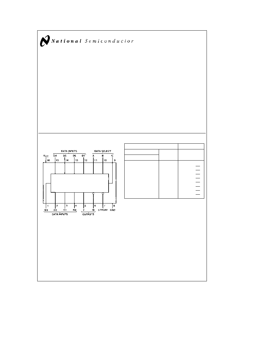
Connection Diagram
Dual-In-Line Package
TL F 6415 ≠ 1
Order Number DM54LS251J DM54LS251W
DM74LS251M or DM74LS251N
See NS Package Number J16A M16A N16E or W16A
Function Table
Inputs
Outputs
Select
Strobe
Y
W
C
B
A
S
X
X
X
H
Z
Z
L
L
L
L
D0
D0
L
L
H
L
D1
D1
L
H
L
L
D2
D2
L
H
H
L
D3
D3
H
L
L
L
D4
D4
H
L
H
L
D5
D5
H
H
L
L
D6
D6
H
H
H
L
D7
D7
H
e
High Logic Level L
e
Low Logic Level
X
e
Don't Care Z
e
High Impedance (Off)
D0 D1
D7
e
The level of the respective D input
TRI-STATE
is a registered trademark of National Semiconductor Corporation
C1995 National Semiconductor Corporation
RRD-B30M105 Printed in U S A
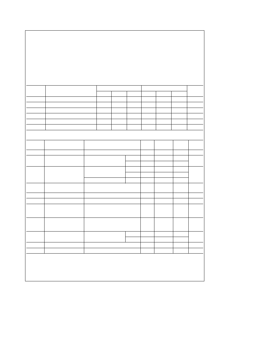
Absolute Maximum Ratings
(Note)
If Military Aerospace specified devices are required
please contact the National Semiconductor Sales
Office Distributors for availability and specifications
Supply Voltage
7V
Input Voltage
7V
Operating Free Air Temperature Range
DM54LS
b
55 C to
a
125 C
DM74LS
0 C to
a
70 C
Storage Temperature Range
b
65 C to
a
150 C
Note
The ``Absolute Maximum Ratings'' are those values
beyond which the safety of the device cannot be guaran-
teed The device should not be operated at these limits The
parametric values defined in the ``Electrical Characteristics''
table are not guaranteed at the absolute maximum ratings
The ``Recommended Operating Conditions'' table will define
the conditions for actual device operation
Recommended Operating Conditions
Symbol
Parameter
DM54LS251
DM74LS251
Units
Min
Nom
Max
Min
Nom
Max
V
CC
Supply Voltage
4 5
5
5 5
4 75
5
5 25
V
V
IH
High Level Input Voltage
2
2
V
V
IL
Low Level Input Voltage
0 7
0 8
V
I
OH
High Level Output Current
b
1
b
2 6
mA
I
OL
Low Level Output Current
12
24
mA
T
A
Free Air Operating Temperature
b
55
125
0
70
C
Electrical Characteristics
over recommended operating free air temperature range (unless otherwise noted)
Symbol
Parameter
Conditions
Min
Typ
Max
Units
(Note 1)
V
I
Input Clamp Voltage
V
CC
e
Min I
I
e b
18 mA
b
1 5
V
V
OH
High Level Output
V
CC
e
Min I
OH
e
Max
DM54
2 4
3 4
V
Voltage
V
IL
e
Max V
IH
e
Min
DM74
2 4
3 1
V
OL
Low Level Output
V
CC
e
Min I
OL
e
Max
DM54
0 25
0 4
Voltage
V
IL
e
Max V
IH
e
Min
DM74
0 35
0 5
V
I
OL
e
12 mA V
CC
e
Min
DM74
0 25
0 4
I
I
Input Current
Max
V
CC
e
Max V
I
e
7V
0 1
mA
Input Voltage
I
IH
High Level Input Current
V
CC
e
Max V
I
e
2 7V
20
m
A
I
IL
Low Level Input Current
V
CC
e
Max V
I
e
0 4V
b
0 4
mA
I
OZH
Off-State Output Current
V
CC
e
Max V
O
e
2 7V
with High Level Output
V
IH
e
Min V
IL
e
Max
20
m
A
Voltage Applied
I
OZL
Off-State Output Current
V
CC
e
Max V
O
e
0 4V
with Low Level Output
V
IH
e
Min V
IL
e
Max
b
20
m
A
Voltage Applied
I
OS
Short Circuit
V
CC
e
Max
DM54
b
20
b
100
mA
Output Current
(Note 2)
DM74
b
20
b
100
I
CC1
Supply Current
V
CC
e
Max (Note 3)
6 1
10
mA
I
CC2
Supply Current
V
CC
e
Max (Note 4)
7 1
12
mA
Note 1
All typicals are at V
CC
e
5V T
A
e
25 C
Note 2
Not more than one output should be shorted at a time and the duration should not exceed one second
Note 3
I
CC1
is measured with the outputs open STROBE grounded and all other inputs at 4 5V
Note 4
I
CC2
is measured with the outputs open and all inputs at 4 5V
2
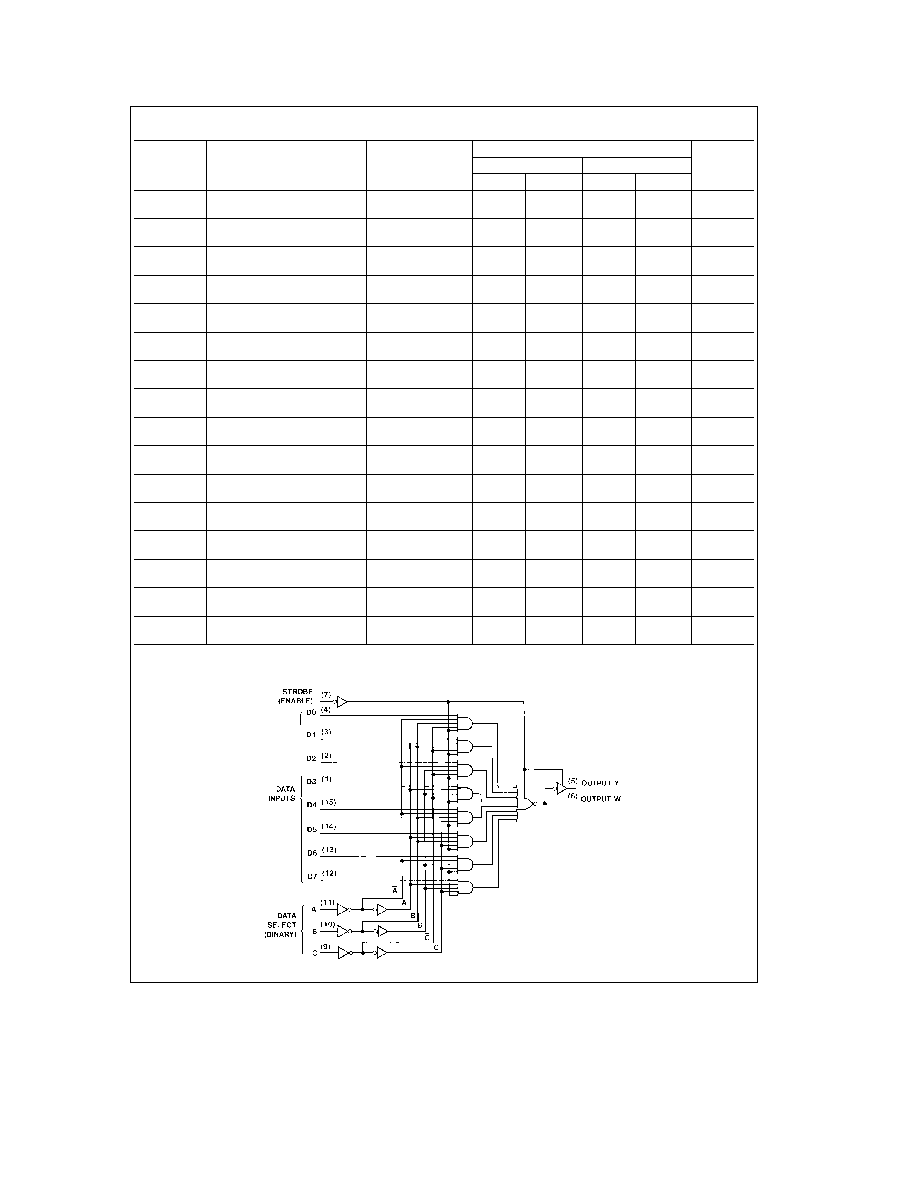
Switching Characteristics
at V
CC
e
5V and T
A
e
25 C (See Section 1 for Test Waveforms and Output Load)
From (Input)
R
L
e
667X
Symbol
Parameter
to (Output)
C
L
e
45 pF
C
L
e
150 pF
Units
Min
Max
Min
Max
t
PLH
Propagation Delay Time
A B C
45
53
ns
Low to High Level Output
(4 Levels) to Y
t
PHL
Propagation Delay Time
A B C
45
53
ns
High to Low Level Output
(4 Levels) to Y
t
PLH
Propagation Delay Time
A B C
33
38
ns
Low to High Level Output
(3 Levels) to W
t
PHL
Propagation Delay Time
A B C
33
42
ns
High to Low Level Output
(3 Levels) to W
t
PLH
Propagation Delay Time
D
28
35
ns
Low to High Level Output
to Y
t
PHL
Propagation Delay Time
D
28
38
ns
High to Low Level Output
to Y
t
PLH
Propagation Delay Time
D
15
25
ns
Low to High Level Output
to W
t
PHL
Propagation Delay Time
D
15
25
ns
High to Low Level Output
to W
t
PZH
Output Enable Time to
Strobe
45
60
ns
High Level Output
to Y
t
PZL
Output Enable Time to
Strobe
40
51
ns
Low Level Output
to Y
t
PHZ
Output Disable Time from
Strobe
45
ns
High Level Output (Note 1)
to Y
t
PLZ
Output Disable Time from
Strobe
25
ns
Low Level Output (Note 1)
to Y
t
PZH
Output Enable Time to
Strobe
27
40
ns
High Level Output
to W
t
PZL
Output Enable Time to
Strobe
40
47
ns
Low Level Output
to W
t
PHZ
Output Disable Time from
Strobe
55
ns
High Level Output (Note 1)
to W
t
PLZ
Output Disable Time from
Strobe
25
ns
Low Level Output (Note 1)
to W
Note 1
C
L
e
5 pF
Logic Diagram
TL F 6415 ≠ 2
3
Physical Dimensions
inches (millimeters)
16-Lead Ceramic Dual-In-Line Package (J)
Order Number DM54LS251J
NS Package Number J16A
4
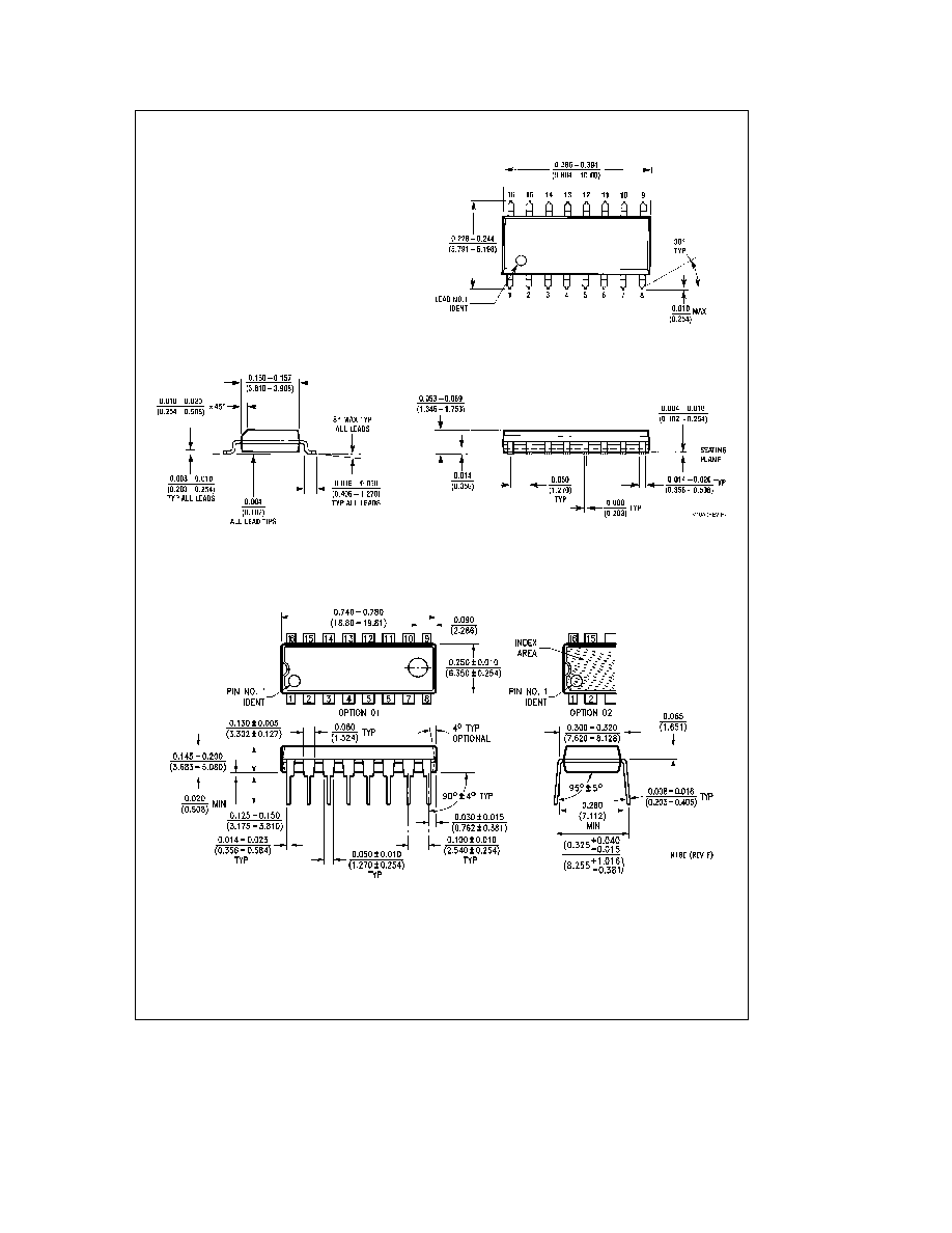
Physical Dimensions
inches (millimeters) (Continued)
16-Lead Small Outline Molded Package (M)
Order Number DM74LS251M
NS Package Number M16A
Molded Dual-In-Line Package (N)
Order Number DM74LS251N
NS Package Number N16E
5