TL F 9827
DM54LS299DM74LS299
8-Input
Universal
ShiftStorage
Register
with
Common
Parallel
IO
Pins
June 1992
DM54LS299 DM74LS299
8-Input Universal Shift Storage Register
with Common Parallel I O Pins
General Description
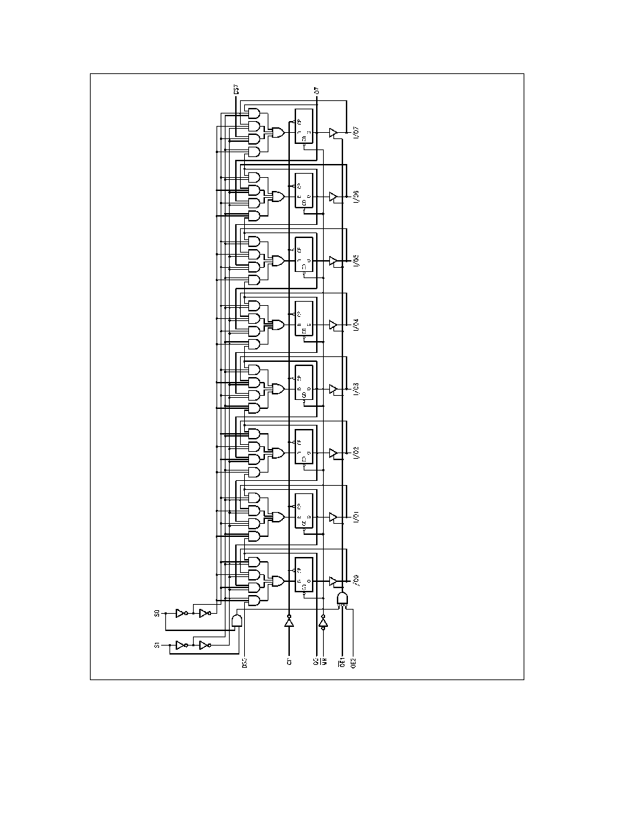
The 'LS299 is an 8-bit universal shift storage register with
TRI-STATE
outputs Four modes of operation are possi-
ble hold (store) shift left shift right and load data The par-
allel load inputs and flip-flop outputs are multiplexed to re-
duce the total number of package pins Separate outputs
are provided for flip-flops Q0 and Q7 to allow easy cascad-
ing A separate active LOW Master Reset is used to reset
the register
Features
Y
Common I O for reduced pin count
Y
Four operation modes shift left shift right load and
store
Y
Separate shift right serial input and shift left serial input
for easy cascading
Y
TRI-STATE outputs for bus oriented applications
Connection Diagram
Dual-In-Line Package
TL F 9827 ≠ 1
Order Number DM54LS299E DM54LS299J DM54LS299W
DM74LS299WM or DM74LS299N
See NS Package Number E20A J20A M20B N20A or W20A
Pin Names
Description
CP
Clock Pulse Input (Active Rising Edge)
D
S0
Serial Data Input for Right Shift
D
S7
Serial Data Input for Left Shift
S0 S1
Mode Select Inputs
MR
Asynchronous Master Reset Input
(Active LOW)
OE1 OE2
TRI-STATE Output Enable Inputs
(Active LOW)
I O0 ≠ I O7
Parallel Data Inputs or TRI-STATE
Parallel Outputs
Q0 ≠ Q7
Serial Outputs
TRI-STATE
is a registered trademark of National Semiconductor Corporation
C1995 National Semiconductor Corporation
RRD-B30M115 Printed in U S A
Absolute Maximum Ratings
(Note)
If Military Aerospace specified devices are required
please contact the National Semiconductor Sales
Office Distributors for availability and specifications
Supply Voltage
7V
Input Voltage
7V
Operating Free Air Temperature Range
DM54
b
55 C to
a
125 C
DM74LS
0 C to
a
70 C
Storage Temperature Range
b
65 C to
a
150 C
Note
The ``Absolute Maximum Ratings'' are those values
beyond which the safety of the device cannot be guaran-
teed The device should not be operated at these limits The
parametric values defined in the ``Electrical Characteristics''
table are not guaranteed at the absolute maximum ratings
The ``Recommended Operating Conditions'' table will define
the conditions for actual device operation
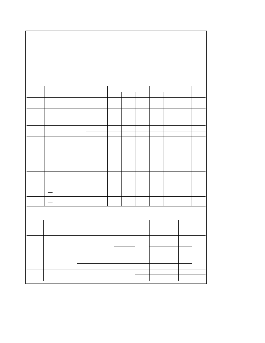
Recommended Operating Conditions
Symbol
Parameter
DM54LS299
DM74LS299
Units
Min
Nom
Max
Min
Nom
Max
V
CC
Supply Voltage
4 5
5
5 5
4 75
5
5 25
V
V
IH
High Level Input Voltage
2
2
V
V
IL
Low Level Input Voltage
0 7
0 8
V
I
OH
High Level Output Current
Q0 Q7
b
0 4
b
0 4
mA
I O0 ≠ I O7
b
2 6
b
2 6
mA
I
OL
Low Level Output Current
Q0 Q7
4
8
mA
I O0 ≠ I O7
12
24
mA
T
A
Free Air Operating Temperature
b
55
125
0
70
C
t
s
(H)
Setup Time HIGH or LOW
24
24
ns
t
s
(L)
S0 or S1 to CP
24
24
t
h
(H)
Hold Time HIGH or LOW
5
0
ns
t
h
(L)
S0 or S1 to CP
5
0
t
s
(H)
Setup Time HIGH or LOW
15
10
ns
t
s
(L)
I O
n
D
S0
D
S7
to CP
15
10
t
h
(H)
Hold Time HIGH or LOW
5
0
ns
t
h
(L)
I O
n
D
S0
D
S7
to CP
5
0
t
w
(H)
CP Pulse Width HIGH or LOW
15
15
ns
t
w
(L)
15
15
t
w
(L)
MR Pulse Width LOW
15
15
ns
t
rec
Recovery Time
10
10
ns
MR to CP
Electrical Characteristics
Over recommended operating free air temperature range (unless otherwise noted)
Symbol
Parameter
Conditions
Min
Typ
Max
Units
(Note 1)
V
I
Input Clamp Voltage
V
CC
e
Min I
I
e b
18 mA
b
1 5
V
V
OH
High Level Output
V
CC
e
Min I
OH
e
Max
DM54
2 5
Voltage
V
IL
e
Max
Q0 Q7
DM74
2 7
3 4
V
I O0 ≠ I O7
2 4
V
OL
Low Level Output
V
CC
e
Min I
OL
e
Max
DM54
0 4
Voltage
V
IH
e
Min
DM74
0 35
0 5
V
I
OL
e
4 mA V
CC
e
Min
DM74
0 25
0 4
I
I
Input Current
Max
V
CC
e
Max V
I
e
10V (DM54)
Inputs
0 1
mA
Input Voltage
V
I
e
7V (DM74)
Sn
0 2
mA
2
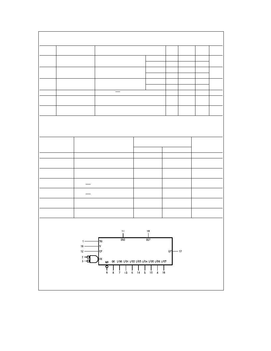
Electrical Characteristics
(Continued)
Over recommended operating free air temperature range (unless otherwise noted)
Symbol
Parameter
Conditions
Min
Typ
Max
Units
(Note 1)
I
IH
High Level Input Current
V
CC
e
Max V
I
e
2 7V
Sn
40
m
A
Inputs
20
m
A
I
IL
Low Level Input Current
V
CC
e
Max V
I
e
0 4V
Sn
b
0 8
mA
Inputs
b
0 4
mA
I
OS
Short Circuit
V
CC
e
Max
Q
0
Q
7
b
20
b
100
mA
Output Current
(Note 2)
I O
0
≠ I O
7
b
30
b
130
I
CC
Supply Current
V
CC
e
Max OE
e
4 5V
60
mA
I
OZH
TRI-STATE Output Off
V
CC
e
Max
40
m
A
Current High
V
O
e
2 7V
I
OZL
TRI-STATE Output Off
V
CC
e
Max
b
400
m
A
Current Low
V
O
e
0 4V
Note 1
All typicals are at V
CC
e
5V T
A
e
25 C
Note 2
Not more than one output should be shorted at a time and the duration should not exceed one second
Switching Characteristics
V
CC
e a
5 0V T
A
e a
25 C (See Section 1 for waveforms and load configurations)
Symbol
Parameter
R
L
e
2 kX
Units
C
L
e
15 pF
Min
Max
f
max
Maximum Input Frequency
35
MHz
t
PLH
Propagation Delay
26
ns
t
PHL
CP to Q0 or Q7
28
t
PLH
Propagation Delay
25
ns
t
PHL
CP to I O
n
35
t
PHL
Propagation Delay
28
ns
MR to Q0 or Q7
t
PHL
Propagation Delay
35
ns
MR to I O
n
t
PZH
Output Enable Time
18
ns
t
PZL
25
t
PHZ
Output Disable Time
15
ns
t
PLZ
20
Logic Symbol
TL F 9827 ≠ 2
V
CC
e
Pin 20
GND
e
Pin 10
3
Functional Description
The 'LS299 contains eight edge-triggered D-type flip-flops
and the interstage logic necessary to perform synchronous
shift left shift right parallel load and hold operations The
type of operation is determined by the S0 and S1 as shown
in the Mode Select Table All flip-flop outputs are brought
out through TRI-STATE buffers to separate I O pins that
also serve as data inputs in the parallel load mode Q0 and
Q7 are also brought out on other pins for expansion in serial
shifting of longer words
A LOW signal on MR overrides the Select and CP inputs
and resets the flip-flops All other state changes are initiated
by the rising edge of the clock Inputs can change when the
clock is in either state provided only that the recommended
setup and hold times relative to the rising edge of CP are
observed
A HIGH signal on either OE1 or OE2 disables the TRI-
STATE buffers and puts the I O pins in the high impedance
state In this condition the shift hold load and reset opera-
tions can still occur The TRI-STATE buffers are also dis-
abled by HIGH signals on both S0 and S1 in preparation for
a parallel load operation
Mode Select Table
Inputs
Response
MR S1 S0 CP
L
X
X
X
Asynchronous Reset Q0 ≠ Q7
e
LOW
H
H
H
L Parallel Load I O
n
x
Q
n
H
L
H
L Shift Right D
S0
x
Q0 Q0
x
Q1 etc
H
H
L
L Shift Left D
S7
x
Q7 Q7
x
Q6 etc
H
L
L
X
Hold
H
e
HIGH Voltage Level
L
e
LOW Voltage Level
X
e
Immaterial
4