 | –≠–ª–µ–∫—Ç—Ä–æ–Ω–Ω—ã–π –∫–æ–º–ø–æ–Ω–µ–Ω—Ç: DM54LS74A | –°–∫–∞—á–∞—Ç—å:  PDF PDF  ZIP ZIP |
TL F 6373
54LS74DM54LS74ADM74LS74A
Dual
Positive-Edge-Triggered
D
Flip-Flops
with
Preset
Clear
and
Complementary
Outputs
June 1989
54LS74 DM54LS74A DM74LS74A
Dual Positive-Edge-Triggered D Flip-Flops
with Preset Clear and Complementary Outputs
General Description
This device contains two independent positive-edge-trig-
gered D flip-flops with complementary outputs The informa-
tion on the D input is accepted by the flip-flops on the posi-
tive going edge of the clock pulse The triggering occurs at a
voltage level and is not directly related to the transition time
of the rising edge of the clock The data on the D input may
be changed while the clock is low or high without affecting
the outputs as long as the data setup and hold times are not
violated A low logic level on the preset or clear inputs will
set or reset the outputs regardless of the logic levels of the
other inputs
Features
Y
Alternate military aerospace device (54LS74) is avail-
able Contact a National Semiconductor Sales Office
Distributor for specifications
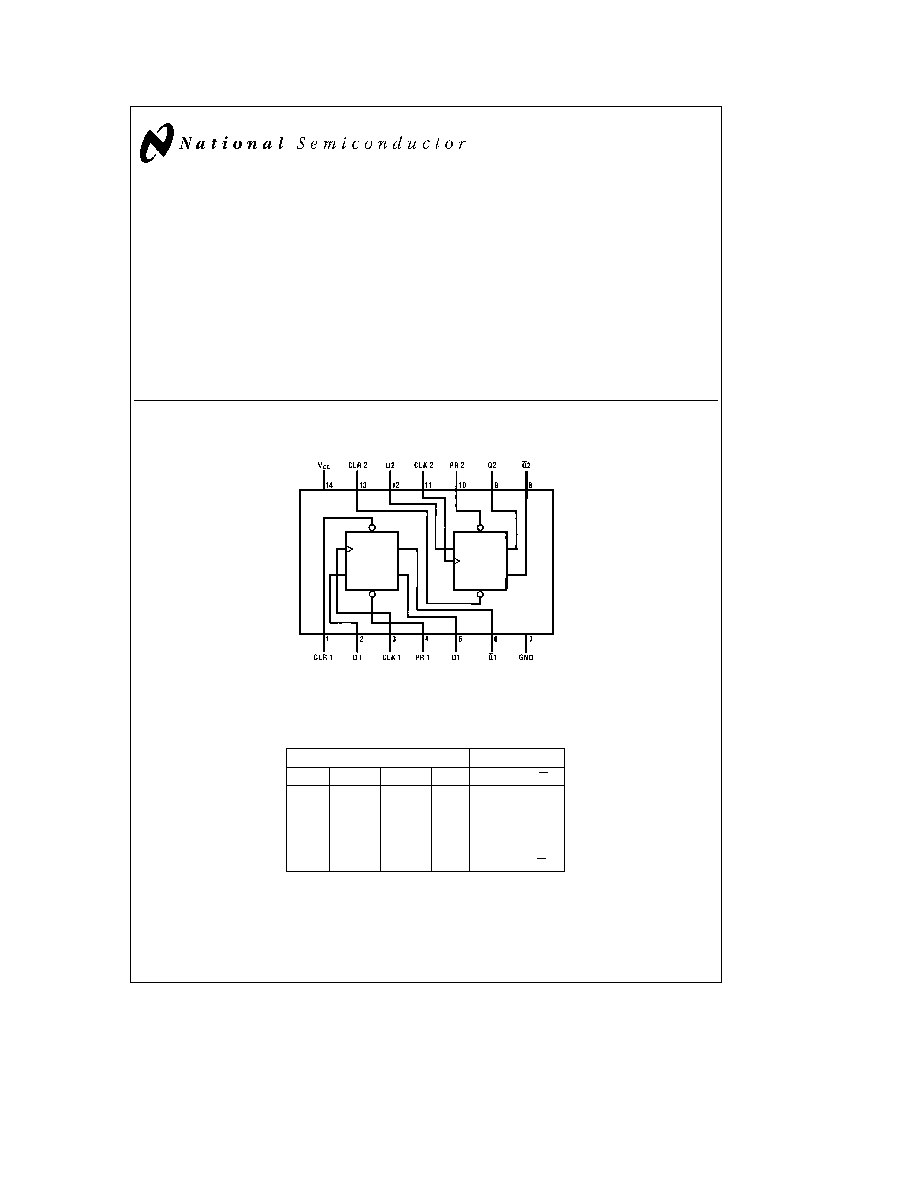
Connection Diagram
Dual-In-Line Package
TL F 6373 ≠ 1
Order Number 54LS74DMQB 54LS74FMQB 54LS74LMQB
DM54LS74AJ DM54LS74AW DM74LS74AM or DM74LS74AN
See NS Package Number E20A J14A M14A N14A or W14B
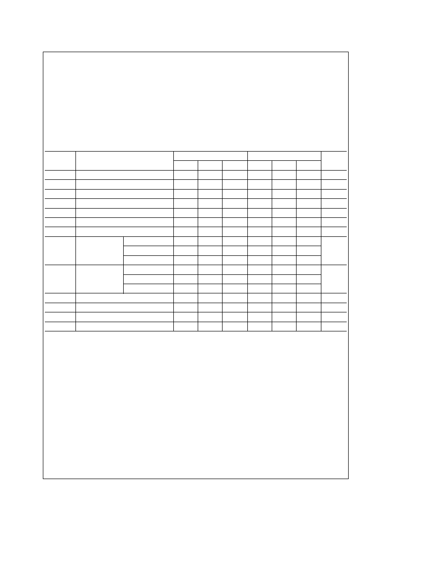
Function Table
Inputs
Outputs
PR
CLR
CLK
D
Q
Q
L
H
X
X
H
L
H
L
X
X
L
H
L
L
X
X
H
H
H
H
u
H
H
L
H
H
u
L
L
H
H
H
L
X
Q
0
Q
0
H
e
High Logic Level
X
e
Either Low or High Logic Level
L
e
Low Logic Level
u
e
Positive-going Transition
e
This configuration is nonstable that is it will not persist when either the preset
and or clear inputs return to their inactive (high) level
Q
0
e
The output logic level of Q before the indicated input conditions were established
C1995 National Semiconductor Corporation
RRD-B30M105 Printed in U S A
Absolute Maximum Ratings
(Note)
If Military Aerospace specified devices are required
please contact the National Semiconductor Sales
Office Distributors for availability and specifications
Supply Voltage
7V
Input Voltage
7V
Operating Free Air Temperature Range
DM54LS and 54LS
b
55 C to
a
125 C
DM74LS
0 C to
a
70 C
Storage Temperature Range
b
65 C to
a
150 C
Note
The ``Absolute Maximum Ratings'' are those values
beyond which the safety of the device cannot be guaran-
teed The device should not be operated at these limits The
parametric values defined in the ``Electrical Characteristics''
table are not guaranteed at the absolute maximum ratings
The ``Recommended Operating Conditions'' table will define
the conditions for actual device operation
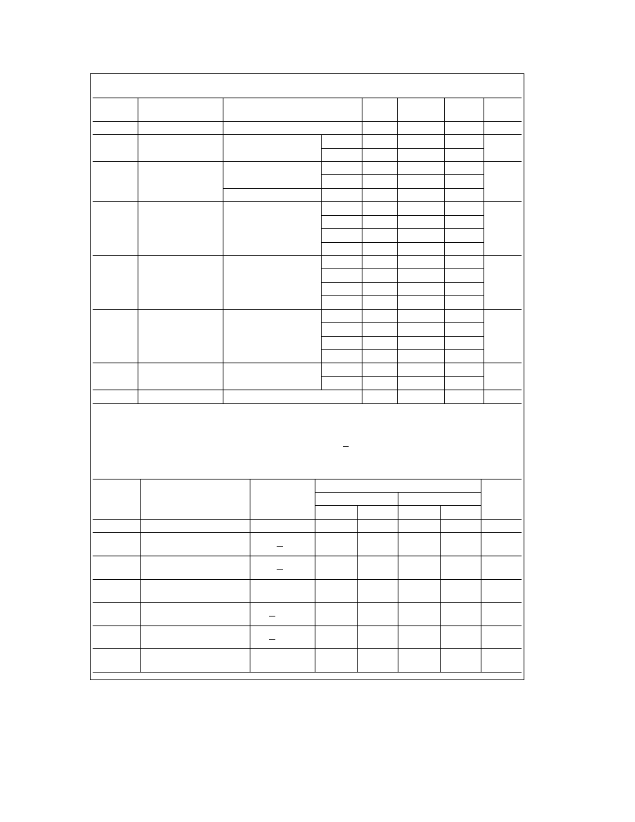
Recommended Operating Conditions
Symbol
Parameter
DM54LS74A
DM74LS74A
Units
Min
Nom
Max
Min
Nom
Max
V
CC
Supply Voltage
4 5
5
5 5
4 75
5
5 25
V
V
IH
High Level Input Voltage
2
2
V
V
IL
Low Level Input Voltage
0 7
0 8
V
I
OH
High Level Output Current
b
0 4
b
0 4
mA
I
OL
Low Level Output Current
4
8
mA
f
CLK
Clock Frequency (Note 2)
0
25
0
25
MHz
f
CLK
Clock Frequency (Note 3)
0
20
0
20
MHz
t
W
Pulse Width
Clock High
18
18
(Note 2)
Preset Low
15
15
ns
Clear Low
15
15
t
W
Pulse Width
Clock High
25
25
(Note 3)
Preset Low
20
20
ns
Clear Low
20
20
t
SU
Setup Time (Notes 1 and 2)
20
u
20
u
ns
t
SU
Setup Time (Notes 1 and 3)
25
u
25
u
ns
t
H
Hold Time (Note 1 and 4)
0
u
0
u
ns
T
A
Free Air Operating Temperature
b
55
125
0
70
C
Note 1
The symbol (
u
) indicates the rising edge of the clock pulse is used for reference
Note 2
C
L
e
15 pF R
L
e
2 kX T
A
e
25 C and V
CC
e
5V
Note 3
C
L
e
50 pF R
L
e
2 kX T
A
e
25 C and V
CC
e
5V
Note 4
T
A
e
25 C and V
CC
e
5V
2
Electrical Characteristics
over recommended operating free air temperature range (unless otherwise noted)
Symbol
Parameter
Conditions
Min
Typ
Max
Units
(Note 1)
V
I
Input Clamp Voltage
V
CC
e
Min I
I
e b
18 mA
b
1 5
V
V
OH
High Level Output
V
CC
e
Min I
OH
e
Max
DM54
2 5
3 4
V
Voltage
V
IL
e
Max V
IH
e
Min
DM74
2 7
3 4
V
OL
Low Level Output
V
CC
e
Min I
OL
e
Max
DM54
0 25
0 4
Voltage
V
IL
e
Max V
IH
e
Min
DM74
0 35
0 5
V
I
OL
e
4 mA V
CC
e
Min
DM74
0 25
0 4
I
I
Input Current
Max
V
CC
e
Max
Data
0 1
Input Voltage
V
I
e
7V
Clock
0 1
mA
Preset
0 2
Clear
0 2
I
IH
High Level Input
V
CC
e
Max
Data
20
Current
V
I
e
2 7V
Clock
20
m
A
Clear
40
Preset
40
I
IL
Low Level Input
V
CC
e
Max
Data
b
0 4
Current
V
I
e
0 4V
Clock
b
0 4
mA
Preset
b
0 8
Clear
b
0 8
I
OS
Short Circuit
V
CC
e
Max
DM54
b
20
b
100
mA
Output Current
(Note 2)
DM74
b
20
b
100
I
CC
Supply Current
V
CC
e
Max (Note 3)
4
8
mA
Note 1
All typicals are at V
CC
e
5V T
A
e
25 C
Note 2
Not more than one output should be shorted at a time and the duration should not exceed one second For devices with feedback from the outputs where
shorting the outputs to ground may cause the outputs to change logic state an equivalent test may be performed where V
O
e
2 25V and 2 125V for DM54 and
DM74 series respectively with the minimum and maximum limits reduced by one half from their stated values This is very useful when using automatic test
equipment
Note 3
With all outputs open I
CC
is measured with CLOCK grounded after setting the Q and Q outputs high in turn
Switching Characteristics
at V
CC
e
5V and T
A
e
25 C (See Section 1 for Test Waveforms and Output Load)
From (Input)
R
L
e
2 kX
Symbol
Parameter
To (Output)
C
L
e
15 pF
C
L
e
50 pF
Units
Min
Max
Min
Max
f
MAX
Maximum Clock Frequency
25
20
MHz
t
PLH
Propagation Delay Time
Clock to
25
35
ns
Low to High Level Output
Q or Q
t
PHL
Propagation Delay Time
Clock to
30
35
ns
High to Low Level Output
Q or Q
t
PLH
Propagation Delay Time
Preset
25
35
ns
Low to High Level Output
to Q
t
PHL
Propagation Delay Time
Preset
30
35
ns
High to Low Level Output
to Q
t
PLH
Propagation Delay Time
Clear
25
35
ns
Low to High Level Output
to Q
t
PHL
Propagation Delay Time
Clear
30
35
ns
High to Low Level Output
to Q
3
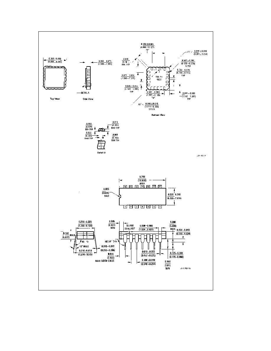
Physical Dimensions
inches (millimeters)
Ceramic Leadless Chip Carrier Package (E)
Order Number 54LS74LMQB
NS Package Number E20A
14-Lead Ceramic Dual-In-Line Package (J)
Order Number 54LS74DMQB or DM54LS74AJ
NS Package Number J14A
4
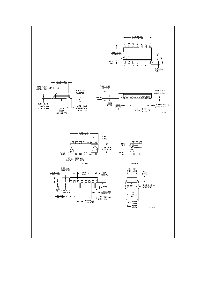
Physical Dimensions
inches (millimeters) (Continued)
14-Lead Small Outline Molded Package (M)
Order Number DM74LS74AM
NS Package Number M14A
14-Lead Molded Dual-In-Line Package (N)
Order Number DM74LS74AN
NS Package Number N14A
5