TL F 6380
DM54LS86DM74LS86
Quad
2-Input
Exclusive-OR
Gates
June 1989
DM54LS86 DM74LS86
Quad 2-Input Exclusive-OR Gates
General Description
This device contains four independent gates each of which
performs the logic exclusive-OR function
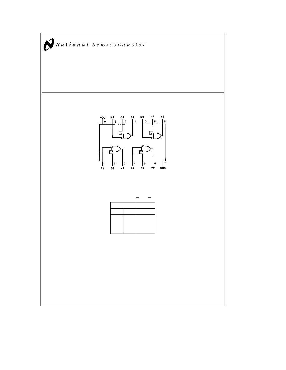
Connection Diagram
Dual-In-Line Package
TL F 6380 ≠ 1
Order Number DM54LS86J DM54LS86W DM74LS86M or DM74LS86N
See NS Package Number J14A M14A N14A or W14B
Function Table
Y
e
A
Z
B
e
AB
a
AB
Inputs
Output
A
B
Y
L
L
L
L
H
H
H
L
H
H
H
L
H
e
High Logic Level
L
e
Low Logic Level
C1995 National Semiconductor Corporation
RRD-B30M105 Printed in U S A
Absolute Maximum Ratings
(Note)
If Military Aerospace specified devices are required
please contact the National Semiconductor Sales
Office Distributors for availability and specifications
Supply Voltage
7V
Input Voltage
7V
Operating Free Air Temperature Range
DM54LS
b
55 C to
a
125 C
DM74LS
0 C to
a
70 C
Storage Temperature Range
b
65 C to
a
150 C
Note
The ``Absolute Maximum Ratings'' are those values
beyond which the safety of the device cannot be guaran-
teed The device should not be operated at these limits The
parametric values defined in the ``Electrical Characteristics''
table are not guaranteed at the absolute maximum ratings
The ``Recommended Operating Conditions'' table will define
the conditions for actual device operation
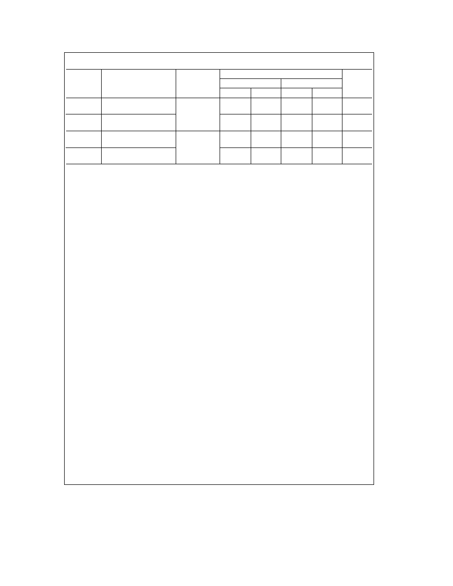
Recommended Operating Conditions
Symbol
Parameter
DM54LS86
DM74LS86
Units
Min
Nom
Max
Min
Nom
Max
V
CC
Supply Voltage
4 5
5
5 5
4 75
5
5 25
V
V
IH
High Level Input Voltage
2
2
V
V
IL
Low Level Input Voltage
0 7
0 8
V
I
OH
High Level Output Current
b
0 4
b
0 4
mA
I
OL
Low Level Output Current
4
8
mA
T
A
Free Air Operating Temperature
b
55
125
0
70
C
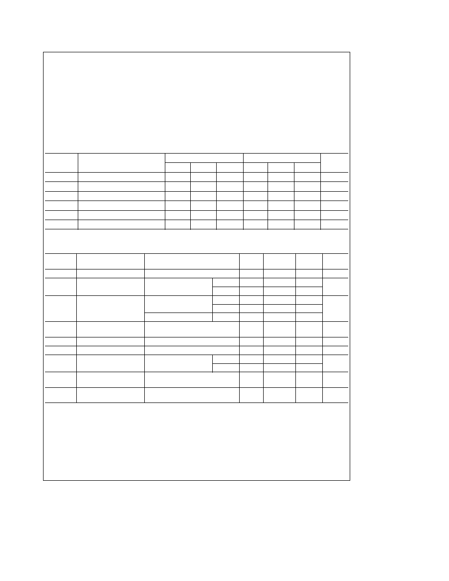
Electrical Characteristics
over recommended operating free air temperature range (unless otherwise noted)
Symbol
Parameter
Conditions
Min
Typ
Max
Units
(Note 1)
V
I
Input Clamp Voltage
V
CC
e
Min I
I
e b
18 mA
b
1 5
V
V
OH
High Level Output
V
CC
e
Min I
OH
e
Max
DM54
2 5
3 4
V
Voltage
V
IL
e
Max V
IH
e
Min
DM74
2 7
3 4
V
OL
Low Level Output
V
CC
e
Min I
OL
e
Max
DM54
0 25
0 4
Voltage
V
IL
e
Max V
IH
e
Min
DM74
0 35
0 5
V
I
OL
e
4 mA V
CC
e
Min
DM74
0 25
0 4
I
I
Input Current
Max
V
CC
e
Max V
I
e
7V
0 2
mA
Input Voltage
I
IH
High Level Input Current
V
CC
e
Max V
I
e
2 7V
40
m
A
I
IL
Low Level Input Current
V
CC
e
Max V
I
e
0 4V
b
0 6
mA
I
OS
Short Circuit
V
CC
e
Max
DM54
b
20
b
100
mA
Output Current
(Note 2)
DM74
b
20
b
100
I
CCH
Supply Current with
V
CC
e
Max
6 1
10
mA
Outputs High
(Note 3)
I
CCL
Supply Current with
V
CC
e
Max
9
15
mA
Outputs Low
(Note 4)
Note 1
All typicals are at V
CC
e
5V T
A
e
25 C
Note 2
Not more than one output should be shorted at a time and the duration should not exceed one second
Note 3
I
CCH
is measured with all outputs open one input at each gate at 4 5V and the other inputs grounded
Note 4
I
CCL
is measured with all outputs open and all inputs grounded
2
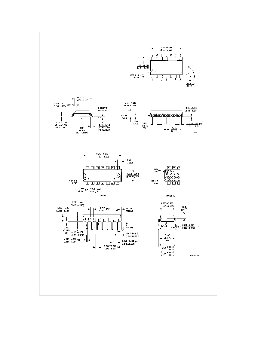
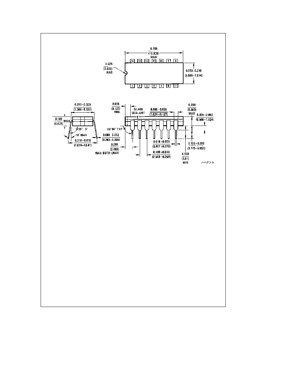
Physical Dimensions
inches (millimeters) (Continued)
14-Lead Small Outline Molded Package (M)
Order Number DM74LS86M
NS Package Number M14A
14-Lead Molded Dual-In-Line Package (N)
Order Number DM74LS86N
NS Package Number N14A
5