 | –≠–ª–µ–∫—Ç—Ä–æ–Ω–Ω—ã–π –∫–æ–º–ø–æ–Ω–µ–Ω—Ç: DM74123N | –°–∫–∞—á–∞—Ç—å:  PDF PDF  ZIP ZIP |
TL F 6539
DM54123DM74123
Dual
Retriggerable
One-Shot
with
Clear
and
Complementary
Outputs
March 1993
DM54123 DM74123 Dual Retriggerable One-Shot with
Clear and Complementary Outputs
General Description
The '123 is a dual retriggerable monostable multivibrator
capable of generating output pulses from a few nano-sec-
onds to extremely long duration up to 100% duty cycle
Each device has three inputs permitting the choice of either
leading-edge or trailing edge triggering Pin (A) is an active-
low transition trigger input and pin (B) is an active-high tran-
sition trigger input A low at the clear (CLR) input terminates
the output pulse which also inhibits triggering An internal
connection from CLR to the input gate makes it possible to
trigger the circuit by a positive-going signal on CLR as
shown in the truth table
To obtain the best and trouble free operation from this de-
vice please read the operating rules as well as the NSC
one ≠ shot application notes carefully and observe recom-
mendations
Features
Y
DC triggered from active-high transition or active-low
transition inputs
Y
Retriggerable to 100% duty cycle
Y
Direct reset terminates output pulse
Y
Compensated for V
CC
and temperature variations
Y
DTL TTL compatible
Y
Input clamp diodes
Functional Description
The basic output pulse width is determined by selection of
an external resistor (R
X
) and capacitor (C
X
) Once triggered
the basic pulse width may be extended by retriggering the
gated active-low transition or active-high transition inputs or
be reduced by use of the active-low transition clear input
Retriggering to 100% duty cycle is possible by application of
an input pulse train whose cycle time is shorter than the
output cycle time such that a continuous ``HIGH'' logic state
is maintained at the ``Q'' output
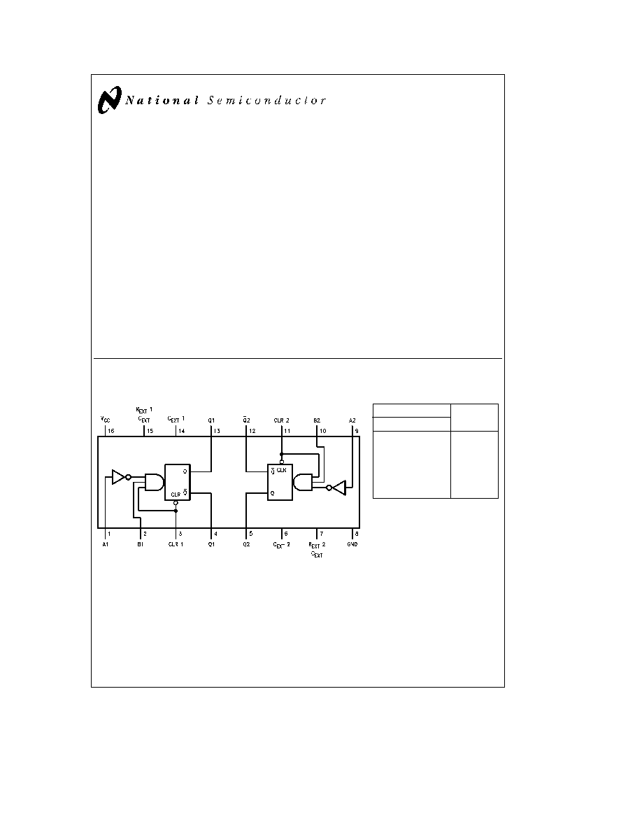
Connection Diagram
Dual-In-Line Package
TL F 6539 ≠ 1
Order Number DM54123J-MIL DM54123W-MIL or DM74123N
See NS Package Number J16A N16A or W16A
Triggering Truth Table
Inputs
Response
A
B
CLR
X
X
L
No Trigger
K
L
X
No Trigger
K
H
H
Trigger
H
L
X
No Trigger
L
L
H
Trigger
L
H
L
Trigger
H
e
HIGH Voltage Level
L
e
LOW Voltage Level
X
e
Immaterial
C1995 National Semiconductor Corporation
RRD-B30M105 Printed in U S A
Absolute Maximum Ratings
(Note)
If Military Aerospace specified devices are required
please contact the National Semiconductor Sales
Office Distributors for availability and specifications
Supply Voltage
7V
Input Voltage
5 5V
Operating Free Air Temperature Range
DM54
b
55 C to
a
100 C
DM74
0 C to
a
70 C
Storage Temperature
b
65 C to
a
150 C
Note
The ``Absolute Maximum Ratings'' are those values
beyond which the safety of the device cannot be guaran-
teed The device should not be operated at these limits The
parametric values defined in the ``Electrical Characteristics''
table are not guaranteed at the absolute maximum ratings
The ``Recommended Operating Conditions'' table will define
the conditions for actual device operation
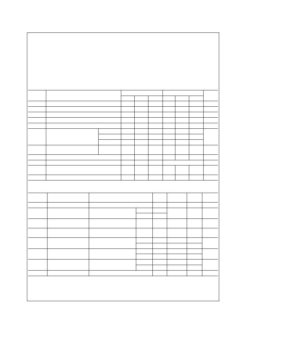
Recommended Operating Conditions
Symbol
Parameter
DM54123
DM74123
Units
Min
Nom
Max
Min
Nom
Max
V
CC
Supply Voltage
4 5
5
5 5
4 75
5
5 25
V
V
IH
High Level Input Voltage
2
2
V
V
IL
Low Level Input Voltage
0 8
0 8
V
I
OH
High Level Output Current
b
0 8
b
0 8
mA
I
OL
Low Level Output Current
16
16
mA
t
W
Pulse Width
A or B High
40
(Note 5)
A or B Low
40
ns
Clear Low
40
T
WQ
Minimum Width of
A or B
80
65
ns
(Min)
Pulse at Q (Note 5)
R
EXT
External Timing Resistor
5
50
kX
C
EXT
External Timing Capacitance
No Restriction
m
F
C
WIRE
Wiring Capacitance
50
pF
at R
EXT
C
EXT
Terminal (Note 5)
T
A
Free Air Operating Temperature
b
55
125
0
70
C
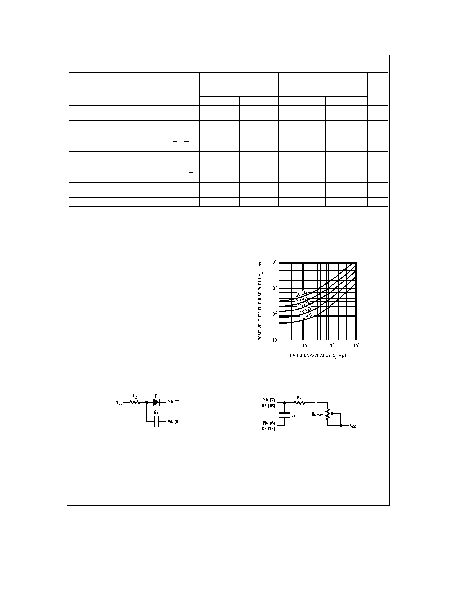
Electrical Characteristics
over recommended operating free air temperature range (unless otherwise noted)
Symbol
Parameter
Conditions
Min
Typ
Max
Units
(Note 1)
V
I
Input Clamp Voltage
V
CC
e
Min I
I
e b
12 mA
b
1 5
V
V
OH
High Level Output
V
CC
e
Min I
OH
e
Max
DM54
2 4
3 4
V
Voltage
V
IL
e
Max V
IH
e
Min
DM74
2 5
V
OL
Low Level Output
V
CC
e
Min I
OL
e
Max
0 2
0 4
V
Voltage
V
IH
e
Min V
IL
e
Max
I
I
Input Current
Max
V
CC
e
Max V
I
e
5 5V
1
mA
Input Voltage
I
IH
High Level Input
V
CC
e
Max
Data
40
m
A
Current
V
I
e
2 4V
Clear
80
I
IL
Low Level Input Current
V
CC
e
Max V
I
e
0 4V
Clear
b
3 2
mA
Data
b
1 6
I
OS
Short Circuit
V
CC
e
Max
DM54
b
10
b
40
mA
Output Current
(Note 2)
DM74
b
10
b
40
I
CC
Supply Current
V
CC
e
Max (Notes 3 and 4)
46
66
mA
Note 1
All typicals are at V
CC
e
5V T
A
e
25 C
Note 2
Not more than one output should be shorted at a time
Note 3
Quiescent I
CC
is measured (after clearing) with 2 4V applied to all clear and A inputs B inputs grounded all outputs open C
EXT
e
0 02 mF and R
EXT
e
25 KX
Note 4
I
CC
is measured in the triggered state with 2 4V applied to all clear and B inputs A inputs grounded all outputs open C
EXT
e
0 02 mF and R
EXT
e
25 kX
Note 5
T
A
e
25 C and V
CC
e
5V
2
Switching Characteristics
at V
CC
e
5V and T
A
e
25 C
DM54123
DM74123
Symbol
Parameter
From (Input)
C
L
e
15 pF R
L
e
400X
C
L
e
15 pF R
L
e
400X
Units
To (Output)
C
EXT
e
0 pF R
EXT
e
5 kX
C
EXT
e
1000 pF R
EXT
e
10 KX
Min
Max
Min
Max
t
PLH
Propagation Delay Time
A to Q
33
33
ns
Low to High Level Output
t
PLH
Propagation Delay Time
B to Q
28
28
ns
Low to High Level Output
t
PHL
Propagation Delay Time
A to Q
40
40
ns
High to Low Level Output
t
PHL
Propagation Delay Time
B to Q
36
36
ns
High to Low Level Output
t
PLH
Propagation Delay Time
Clear to Q
40
40
ns
Low to High Level Output
t
PHL
Propagation Delay Time
Clear to Q
27
27
ns
High to Low Level Output
t
W(out)
Output Pulse Width
A or B to Q
3 08
3 76
3 08
3 76
m
s
C
ECT
e
1000 pF R
EXT
e
10 kX
Operating Rules
1 An external resistor (R
X
) and external capacitor (C
X
) are
required for proper operation The value of C
X
may vary
from 0 to any necessary value For small time constants
high-grade mica glass polypropylene polycarbonate or
polystyrene material capacitors may be used For large
time constants use tantalum or special aluminum capaci-
tors If the timing capacitors have leakages approaching
100 nA or if stray capacitance from either terminal to
ground is greater than 50 pF the timing equations may
not represent the pulse width the device generates
2 When an electrolytic capacitor is used for C
X
a switching
diode is often required for standard TTL one-shots to pre-
vent high inverse leakage current
(Figure 1) However its
use in general is not recommended with retriggerable op-
eration
3 The output pulse width (T
W
) for C
X
l
1000 pF is defined
as follows
T
W
e
K R
X
C
X
(1
a
0 7 R
X
)
where R
X
is in Kilo-ohm
C
X
is in pico Farad
T
W
is in nano second
K
0 28
TL F 6539 ≠ 3
FIGURE 1
4 For C
X
k
1000 pF see
Figure 2 for T
W
vs C
X
family
curves with R
X
as a parameter
Pulse Width vs R
X
and C
X
TL F 6539 ≠ 4
FIGURE 2
5 To obtain variable pulse width by remote trimming the
following circuit is recommended
TL F 6539 ≠ 5
Note
``R
remote
'' should be as close to the one-shot as possible
FIGURE 3
3
Operating Rules
(Continued)
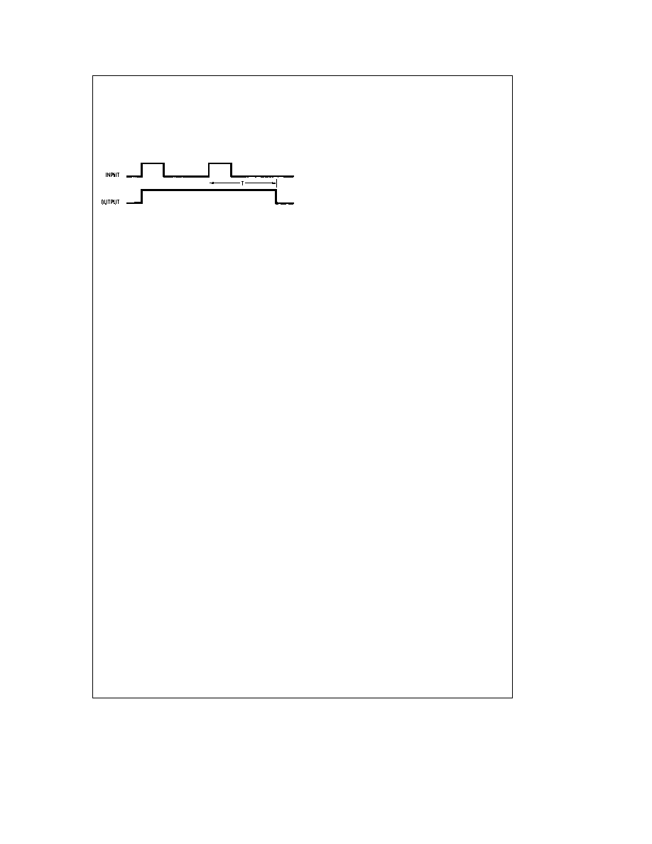
6 The retriggerable pulse width is calculated as shown be-
low
T
e
T
W
a
t
PLH
e
K
c
R
X
c
C
X
a
t
PLH
The retriggered pulse width is equal to the pulse width
plus a delay time period
(Figure 4)
TL F 6539 ≠ 6
FIGURE 4
7 Under any operating condition C
X
and R
X
must be kept
as close to the one-shot device pins as possible to mini-
mize stray capacitance to reduce noise pick-up and to
reduce I
c
R and Ldi dt voltage developed along their
connecting paths If the lead length from C
X
to pins (6)
and (7) or pins (14) and (15) is greater than 3 cm for
example the output pulse width might be quite different
from values predicted from the appropriate equations A
non-inductive and low capacitive path is necessary to en-
sure complete discharge of C
X
in each cycle of its opera-
tion so that the output pulse width will be accurate
8 V
CC
and ground wiring should conform to good high-fre-
quency standards and practices so that switching tran-
sients on the V
CC
and ground return leads do not cause
interaction between one-shots A 0 01 mF to 0 10 mF by-
pass capacitor (disk ceramic or monolithic type) from V
CC
to ground is necessary on each device Furthermore the
bypass capacitor should be located as close to the V
CC
pin as space permits
For further detailed device characteristics and output performance
please refer to the NSC one-shot application note AN-366
4
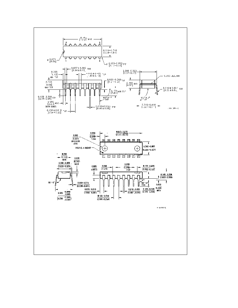
Physical Dimensions
inches (millimeters)
Ceramic Dual-In-Line Package (J)
Order Number DM54123J-MIL
NS Package Number J16A
Molded Dual-In-Line Package (N)
Order Number DM74123N
NS Package Number N16A
5