TL F 6551
DM54161DM74161DM74163
Synchronous
4-Bit
Counters
October 1992
DM54161 DM74161 DM74163
Synchronous 4-Bit Counters
General Description
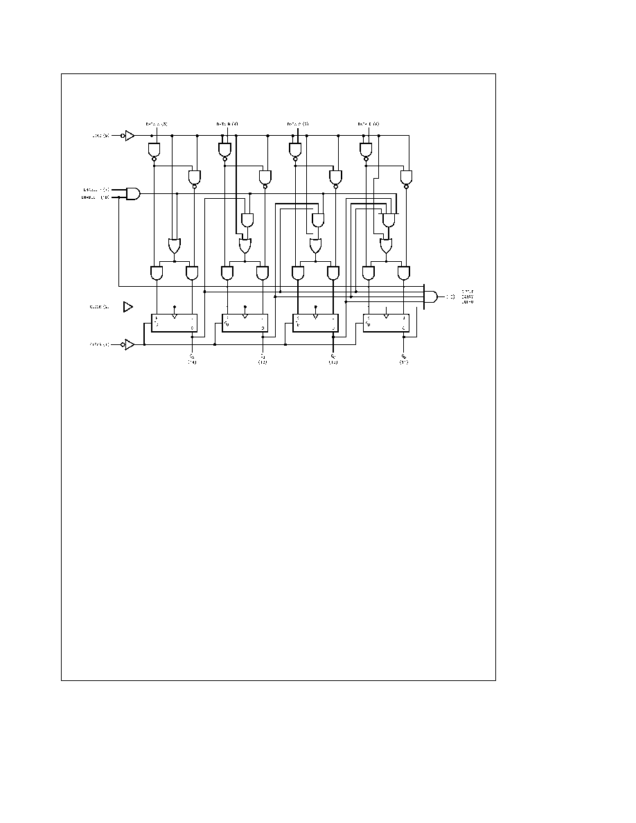
These synchronous presettable counters feature an inter-
nal carry look-ahead for application in high-speed counting
designs The 161 and 163 are 4-bit binary counters The
carry output is decoded by means of a NOR gate thus pre-
venting spikes during the normal counting mode of opera-
tion Synchronous operation is provided by having all flip-
flops clocked simultaneously so that the outputs change co-
incident with each other when so instructed by the count-
enable inputs and internal gating This mode of operation
eliminates the output counting spikes which are normally
associated with asynchronous (ripple clock) counters A
buffered clock input triggers the four flip-flops on the rising
(positive-going) edge of the clock input waveform
These counters are fully programmable that is the outputs
may be preset to either level As presetting is synchronous
setting up a low level at the load input disables the counter
and causes the outputs to agree with the setup data after
the next clock pulse regardless of the levels of the enable
input The clear function for the 161 is asynchronous and a
low level at the clear input sets all four of the flip-flop out-
puts low regardless of the levels of clock load or enable
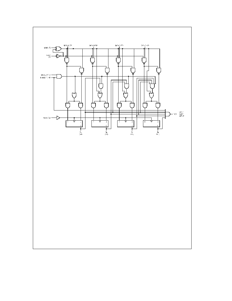
inputs The clear function for the 163 is synchronous and a
low level at the clear input sets all four of the flip-flop out-
puts low after the next clock pulse regardless of the levels
of the enable inputs This synchronous clear allows the
count length to be modified easily as decoding the maxi-
mum count desired can be accomplished with one
external NAND gate The gate output is connected to the
clear input to synchronously clear the counter to all low out-
puts Low-to-high transitions at the clear input of the 163 are
also permissible regardless of the logic levels on the clock
enable or load inputs
The carry look-ahead circuitry provides for cascading coun-
ters for n-bit synchronous applications without additional
gating Instrumental in accomplishing this function are two
count-enable inputs and a ripple carry output Both count-
enable inputs (P and T) must be high to count and input T is
fed forward to enable the ripple carry output The ripple car-
ry output thus enabled will produce a high-level output pulse
with a duration approximately equal to the high-level portion
of the Q
A
output This high-level overflow ripple carry pulse
can be used to enable successive cascaded stages High-
to-low-level transitions at the enable P or T inputs of the 161
through 163 may occur regardless of the logic level on the
clock
Features
Y
Synchronously programmable
Y
Internal look-ahead for fast counting
Y
Carry output for n-bit cascading
Y
Synchronous counting
Y
Load control line
Y
Diode-clamped inputs
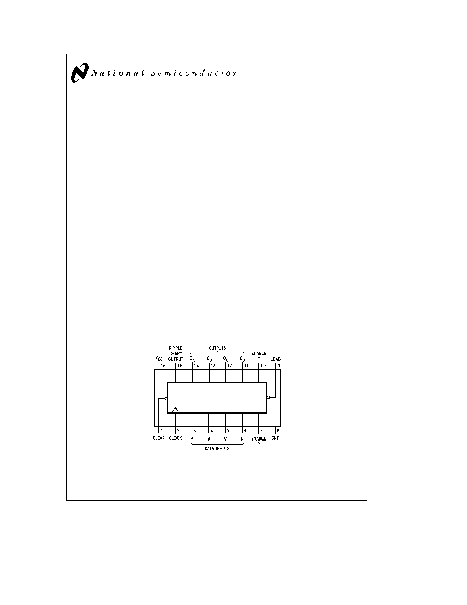
Connection Diagram
Dual-In-Line Package
TL F 6551 1
Order Number DM54161J DM54161W
DM74161N or DM74163N
See NS Package Number J16A N16E or W16A
C1995 National Semiconductor Corporation
RRD-B30M105 Printed in U S A
Absolute Maximum Ratings
(Note)
If Military Aerospace specified devices are required
please contact the National Semiconductor Sales
Office Distributors for availability and specifications
Supply Voltage
7V
Input Voltage
5 5V
Operating Free Air Temperature Range
DM54
b
55 C to
a
125 C
DM74
0 C to
a
70 C
Storage Temperature Range
b
65 C to
a
150 C
Note
The ``Absolute Maximum Ratings'' are those values
beyond which the safety of the device cannot be guaran-
teed The device should not be operated at these limits The
parametric values defined in the ``Electrical Characteristics''
table are not guaranteed at the absolute maximum ratings
The ``Recommended Operating Conditions'' table will define
the conditions for actual device operation
Recommended Operating Conditions
Symbol
Parameter
DM54161
DM74161 and 163
Units
Min
Nom
Max
Min
Nom
Max
V
CC
Supply Voltage
4 5
5
5 5
4 75
5
5 25
V
V
IH
High Level Input Voltage
2
2
V
V
IL
Low Level Input Voltage
0 8
0 8
V
I
OH
High Level Output Current
b
0 8
b
0 8
mA
I
OL
Low Level Output Current
16
16
mA
f
CLK
Clock Frequency (Note 6)
0
25
0
25
MHz
t
W
Pulse Width
Clock
25
25
ns
(Note 6)
Clear
20
20
t
SU
Setup Time
Data
20
20
(Note 6)
Enable P
34
34
ns
Load
25
25
Clear (Note 5)
20
20
t
H
Hold Time (Note 6)
0
0
ns
T
A
Free Air Operating Temperature
b
55
125
0
70
C
Electrical Characteristics
Over recommended operating free air temperature range (unless otherwise noted)
Symbol
Parameter
Conditions
Min
Typ
Max
Units
(Note 1)
V
I
Input Clamp Voltage
V
CC
e
Min I
I
e b
12 mA
b
1 5
V
V
OH
High Level Output
V
CC
e
Min I
OH
e
Max
2 4
3 4
V
Voltage
V
IL
e
Max V
IH
e
Min
V
OL
Low Level Output
V
CC
e
Min I
OL
e
Max
0 2
0 4
V
Voltage
V
IH
e
Min V
IL
e
Max
I
I
Input Current
Max
V
CC
e
Max V
I
e
5 5V
1
mA
Input Voltage
I
IH
High Level Input
V
CC
e
Max
Enable T
80
Current
V
I
e
2 4V
Clock
80
m
A
Others
40
I
IL
Low Level Input
V
CC
e
Max
Enable T
b
3 2
Current
V
I
e
0 4V
Clock
b
3 2
mA
Others
b
1 6
2
Electrical Characteristics
Over recommended operating free air temperature range (unless otherwise noted) (Continued)
Symbol
Parameter
Conditions
Min
Typ
Max
Units
(Note 1)
I
OS
Short Circuit
V
CC
e
Max
DM54
b
20
b
57
mA
Output Current
(Note 2)
DM74
b
20
b
57
I
CCH
Supply Current
V
CC
e
Max
DM54
85
mA
with Outputs High
(Note 3)
DM74
59
94
I
CCL
Supply Current
V
CC
e
Max
DM54
91
mA
with Outputs Low
(Note 4)
DM74
63
101
Note 1
All typicals are at V
CC
e
5V T
A
e
25 C
Note 2
Not more than one output should be shorted at a time
Note 3
I
CCH
is measured with the LOAD high then again with the LOAD low with all inputs high and all outputs open
Note 4
I
CCL
is measured with the CLOCK high then again with the CLOCK input low with all inputs low and all outputs open
Note 5
Applies to 163 which has synchronous clear inputs
Note 6
T
A
e
25 C and V
CC
e
5V
Switching Characteristics
at V
CC
e
5V and T
A
e
25 C (See Section 1 for Test Waveforms and Output Load)
Symbol
Parameter
From (Input)
R
L
e
400X C
L
e
15 pF
Units
To (Output)
Min
Max
f
MAX
Maximum Clock
25
MHz
Frequency
t
PLH
Propagation Delay Time
Clock to
35
ns
Low to High Level Output
Ripple Carry
t
PHL
Propagation Delay Time
Clock to
35
ns
High to Low Level Output
Ripple Carry
t
PLH
Propagation Delay Time
Clock
20
ns
Low to High Level Output
(Load High) to Q
t
PHL
Propagation Delay Time
Clock
23
ns
High to Low Level Output
(Load High) to Q
t
PLH
Propagation Delay Time
Clock
25
ns
Low to High Level Output
(Load Low) to Q
t
PHL
Propagation Delay Time
Clock
29
ns
High to Low Level Output
(Load Low) to Q
t
PLH
Propagation Delay Time
Enable T to
16
ns
Low to High Level Output
Ripple Carry
t
PHL
Propagation Delay Time
Enable T to
16
ns
High to Low Level Output
Ripple Carry
t
PHL
Propagation Delay Time
Clear (Note 7)
38
ns
High to Low Level Output
to Q
Note 7
Propagation delay for clearing is measured from the clear input for the 161 or from the clock input transition for the 163
3