 | –≠–ª–µ–∫—Ç—Ä–æ–Ω–Ω—ã–π –∫–æ–º–ø–æ–Ω–µ–Ω—Ç: DM7495N | –°–∫–∞—á–∞—Ç—å:  PDF PDF  ZIP ZIP |
TL F 6534
5495ADM7495
4-Bit
Parallel
Access
Shift
Registers
June 1989
5495A DM7495
4-Bit Parallel Access Shift Registers
General Description
These 4-bit registers feature parallel and serial inputs paral-
lel outputs mode control and two clock inputs The regis-
ters have three modes of operation
Parallel (broadside) load
Shift right (the direction Q
A
toward Q
D
)
Shift left (the direction Q
D
toward Q
A
)
Parallel loading is accomplished by applying the four bits of
data and taking the mode control input high The data is
loaded into the associated flip-flops and appears at the out-
puts after the high-to-low transition of the clock-2 input Dur-
ing loading the entry of serial data is inhibited
Shift right is accomplished on the high-to-low transition of
clock 1 when the mode control is low shift left is accom-
plished on the high-to-low transition of clock 2 when the
mode control is high by connecting the output of each flip-
flop to the parallel input of the previous flip-flop (Q
D
to input
C etc ) and serial data is entered at input D The clock input
may be applied simultaneously to clock 1 and clock 2 if both
modes can be clocked from the same source
Changes at the mode control input should normally be
made while both clock inputs are low however conditions
described in the last three lines of the truth table will also
ensure that register contents are protected
Features
Y
Typical maximum clock frequency 36 MHz
Y
Typical power dissipation 250 mW
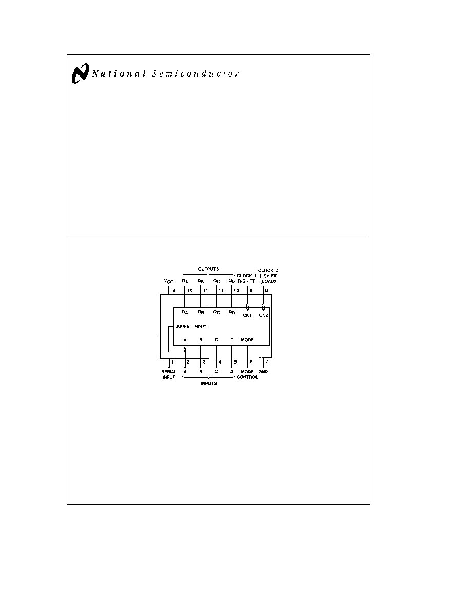
Connection Diagram
Dual-In-Line Package
TL F 6534 ≠ 1
Order Number 5495ADMQB 5495AFMQB or DM7495N
See NS Package Number J14A N14A or W14B
C1995 National Semiconductor Corporation
RRD-B30M105 Printed in U S A
Absolute Maximum Ratings
(Note)
If Military Aerospace specified devices are required
please contact the National Semiconductor Sales
Office Distributors for availability and specifications
Supply Voltage
7V
Input Voltage
5 5V
Operating Free Air Temperature Range
54A
b
55 C to
a
125 C
DM74
0 C to
a
70 C
Storage Temperature Range
b
65 C to
a
150 C
Note
The ``Absolute Maximum Ratings'' are those values
beyond which the safety of the device cannot be guaran-
teed The device should not be operated at these limits The
parametric values defined in the ``Electrical Characteristics''
table are not guaranteed at the absolute maximum ratings
The ``Recommended Operating Conditions'' table will define
the conditions for actual device operation
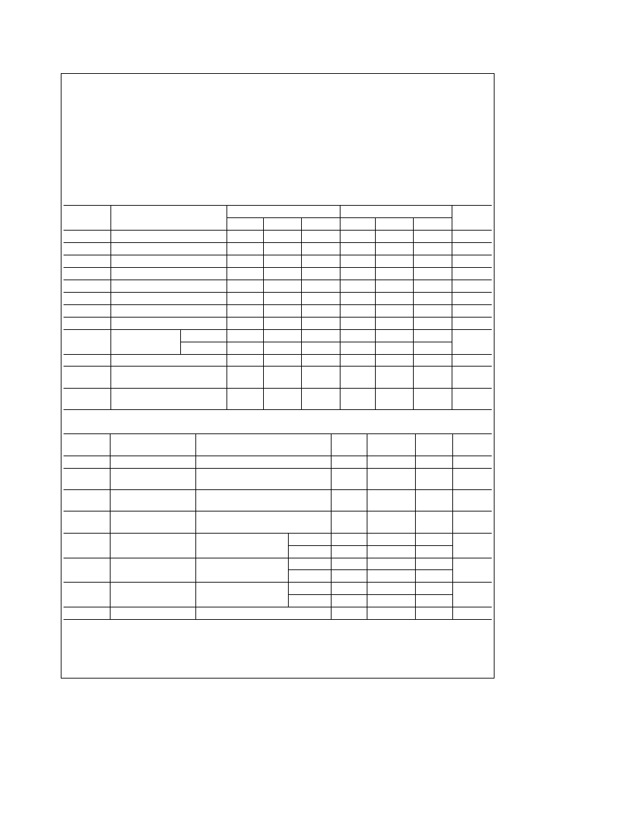
Recommended Operating Conditions
Symbol
Parameter
5495A
DM7495
Units
Min
Nom
Max
Min
Nom
Max
V
CC
Supply Voltage
4 5
5
5 5
4 75
5
5 25
V
V
IH
High Level Input Voltage
2
2
V
V
IL
Low Level Input Voltage
0 8
0 8
V
I
OH
High Level Output Current
b
0 8
b
0 8
mA
I
OL
Low Level Output Current
16
16
mA
f
CLK
Clock Frequency (Note 4)
0
25
0
25
MHz
t
W
Clock Pulse Width (Note 4)
15
11
15
ns
t
SU
Data Setup Time (Note 4)
20
10
20
10
ns
t
EN
Time to Enable
Clock 1
20
20
ns
Clock (Note 4)
Clock 2
15
15
t
H
Data Hold Time (Note 4)
0
b
10
0
b
10
ns
t
IN
Time to Inhibit Clock 1
10
10
ns
or Clock 2 (Note 4)
T
A
Free Air Operating
b
55
125
0
70
C
Temperature
Electrical Characteristics
over recommended operating free air temperature range (unless otherwise noted)
Symbol
Parameter
Conditions
Min
Typ
Max
Units
(Note 1)
V
I
Input Clamp Voltage
V
CC
e
Min I
I
e b
12 mA
b
1 5
V
V
OH
High Level Output
V
CC
e
Min I
OH
e
Max
2 4
3 4
V
Voltage
V
IL
e
Max V
IH
e
Min
V
OL
Low Level Output
V
CC
e
Min I
OL
e
Max
0 2
0 4
V
Voltage
V
IH
e
Min V
IL
e
Max
I
I
Input Current
Max
V
CC
e
Max V
I
e
5 5V
1
mA
Input Voltage
I
IH
High Level Input
V
CC
e
Max
Mode
80
m
A
Current
V
I
e
2 4V
Others
40
I
IL
Low Level Input
V
CC
e
Max
Mode
b
3 2
mA
Current
V
I
e
0 4V
Others
b
1 6
I
OS
Short Circuit
V
CC
e
Max
DM54
b
18
b
57
mA
Output Current
(Note 2)
DM74
b
18
b
57
I
CC
Supply Current
V
CC
e
Max (Note 3)
50
75
mA
Note 1
All typicals are at V
CC
e
5V T
A
e
25 C
Note 2
Not more than one output should be shorted at a time
Note 3
I
CC
is measured with all outputs and serial input open A B C and D inputs grounded Mode Control at 4 5V and a momentary 3V then ground applied to
both clock inputs
Note 4
T
A
e
25 C and V
CC
e
5V
2
Switching Characteristics
at V
CC
e
5V and T
A
e
25 C (See Section 1 for Test Waveforms and Output Load)
Symbol
Parameter
From (Input)
R
L
e
400X C
L
e
15 pF
Units
To (Output)
Min
Max
f
MAX
Maximum Clock Frequency
25
MHz
t
PHL
Propagation Delay Time
Clock to
35
ns
High to Low Level Output
Output
t
PLH
Propagation Delay Time
Clock to
35
ns
Low to High Level Output
Output
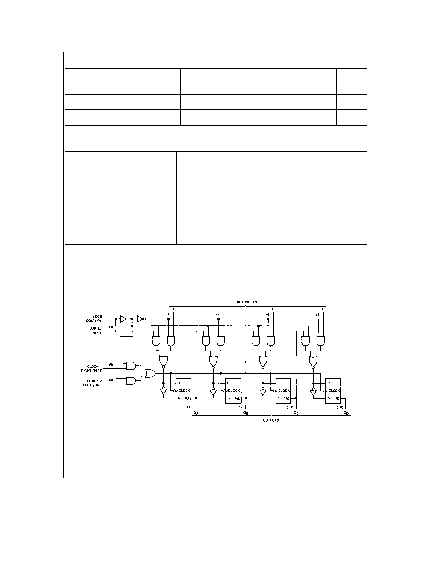
Function Table
Inputs
Outputs
Mode
Clocks
Serial
Parallel
Q
A
Q
B
Q
C
Q
D
Control
2(L)
1(R)
A
B
C
D
H
H
X
X
X
X
X
X
Q
A0
Q
B0
Q
C0
Q
D0
H
v
X
X
a
b
c
d
a
b
c
d
H
v
X
X
Q
B
Q
C
Q
D
d
Q
Bn
Q
Cn
Q
Dn
d
L
L
H
X
X
X
X
X
Q
A0
Q
B0
Q
C0
Q
D0
L
X
v
H
X
X
X
X
H
Q
An
Q
Bn
Q
Cn
L
X
v
L
X
X
X
X
L
Q
An
Q
Bn
Q
Cn
u
L
L
X
X
X
X
X
Q
A0
Q
B0
Q
C0
Q
D0
v
L
L
X
X
X
X
X
Q
A0
Q
B0
Q
C0
Q
D0
v
L
H
X
X
X
X
X
Q
A0
Q
B0
Q
C0
Q
D0
u
H
L
X
X
X
X
X
Q
A0
Q
B0
Q
C0
Q
D0
u
H
H
X
X
X
X
X
Q
A0
Q
B0
Q
C0
Q
D0
Shifting left requires external connection of Q
B
to A Q
C
to B Q
D
to C Serial data is entered at input D
H
e
High Level (Steady State) L
e
Low Level (Steady State) X
e
Don't Care (Any input including transitions)
v
e
Transition from high to low level
u
e
Transition from low to high level
a b c d
e
The level of steady state input at inputs A B C or D respectively
Q
A0
Q
B0
Q
C0
Q
D0
e
The level of Q
A
Q
B
Q
C
Q
D
respectively before the indicated steady state input conditions were established
Q
An
Q
Bn
Q
Cn
Q
Dn
e
The level of Q
A
Q
B
Q
C
Q
D
respectively before the most recent
v
transition of the clock
Logic Diagram
TL F 6534 ≠ 2
3

4
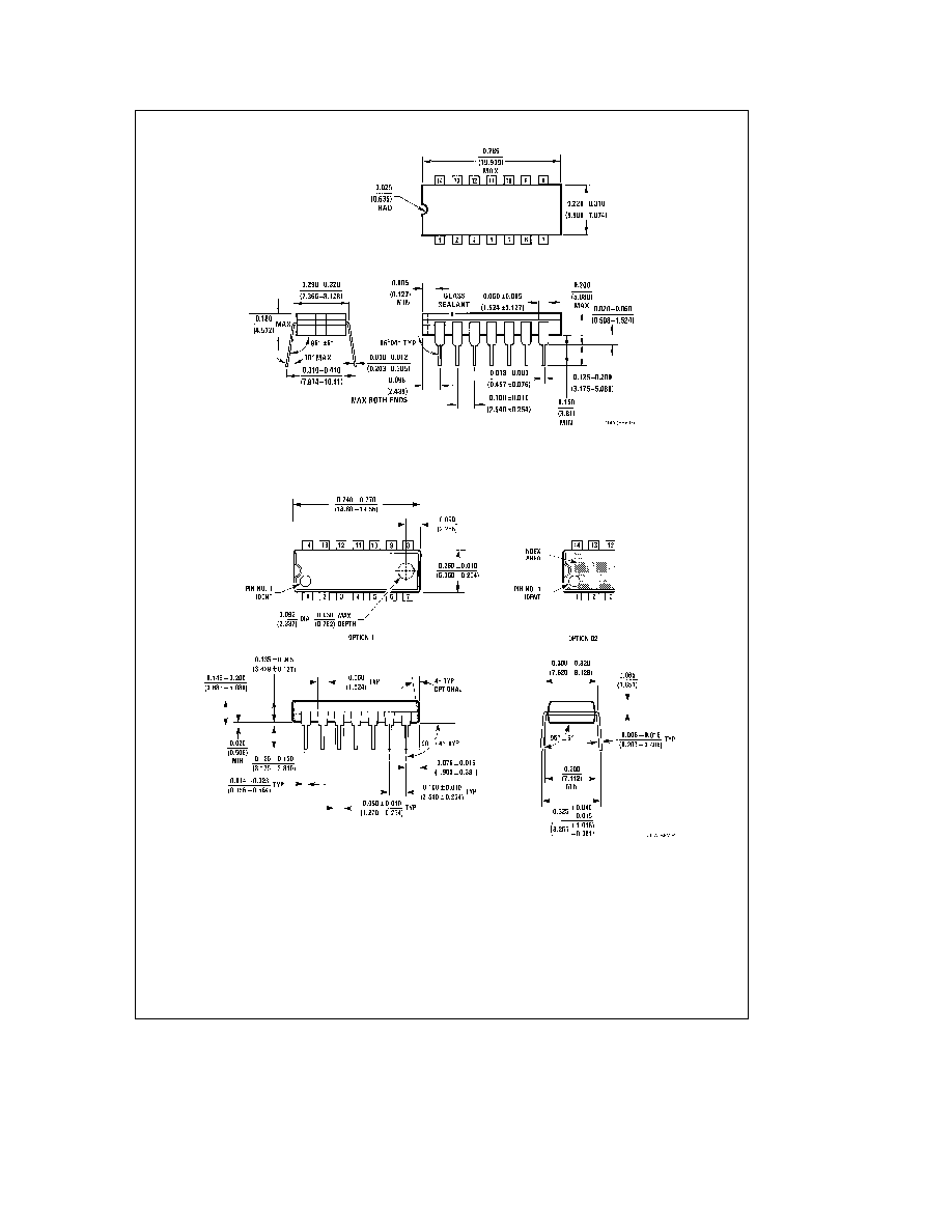
Physical Dimensions
inches (millimeters)
14-Lead Ceramic Dual-In-Line Package (J)
Order Number 5495ADMQB
NS Package Number J14A
14-Lead Molded Dual-In-Line Package (N)
Order Number DM7495N
NS Package Number N14A
5