 | –≠–ª–µ–∫—Ç—Ä–æ–Ω–Ω—ã–π –∫–æ–º–ø–æ–Ω–µ–Ω—Ç: DM7497 | –°–∫–∞—á–∞—Ç—å:  PDF PDF  ZIP ZIP |
TL F 9780
5497DM7497
Synchronous
Modulo-64
Bit
Rate
Multiplier
June 1989
5497 DM7497
Synchronous Modulo-64 Bit Rate Multiplier
General Description
The '97 contains a synchronous 6-stage binary counter and
six decoding gates that serve to gate the clock through to
the output at a sub-multiple of the input frequency The out-
put pulse rate relative to the clock frequency is determined
by signals applied to the Select (S0 ≠ S5) inputs Both true
and complement outputs are available along with an enable
input for each A Count Enable input and a Terminal Count
output are provided for cascading two or more packages
An asynchronous Master Reset input prevents counting and
resets the counter
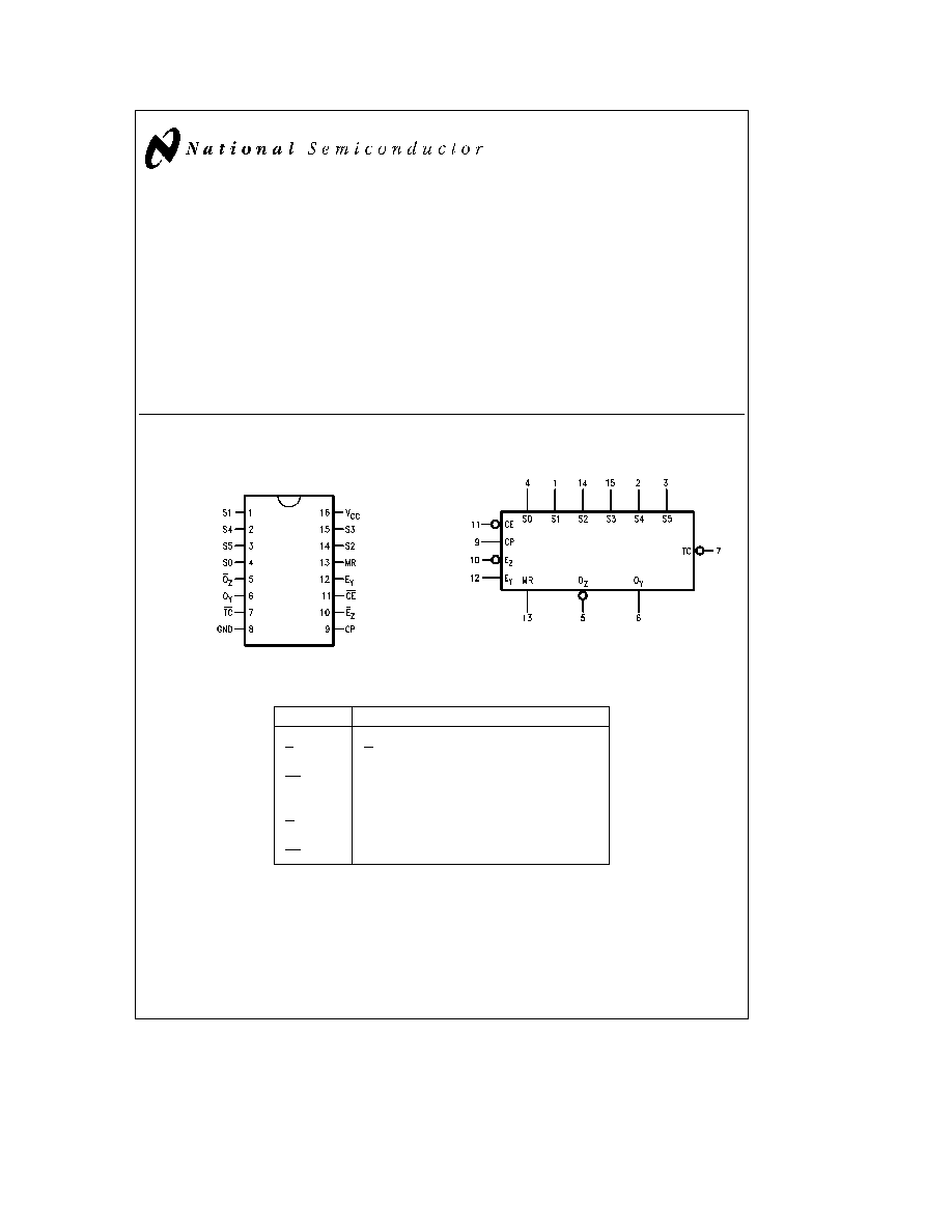
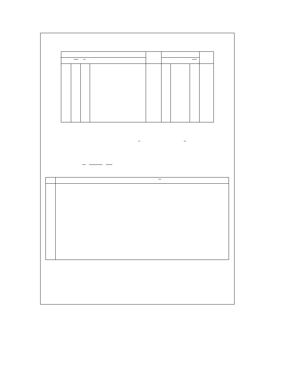
Connection Diagram
Dual-In-Line Package
TL F 9780 ≠ 1
Order Number 5497DMQB 5497FMQB or DM7497N
See NS Package Number J16A N16E or W16A
Logic Symbol
TL F 9780 ≠ 2
V
CC
e
Pin 16
GND
e
Pin 8
Pin Names
Description
S0 ≠ S5
Rate Select Inputs
E
Z
O
Z
Enable Input (Active LOW)
E
Y
O
Y
Enable Input
CE
Count Enable Input (Active LOW)
CP
Clock Pulse Input (Active Rising Edge)
MR
Asynchronous Master Reset Input (Active HIGH)
O
Z
Gated Clock Output (Active LOW)
O
y
Complement Output (Active HIGH)
TC
Terminal Count Output (Active LOW)
C1995 National Semiconductor Corporation
RRD-B30M115 Printed in U S A
Absolute Maximum Ratings
(Note)
If Military Aerospace specified devices are required
please contact the National Semiconductor Sales
Office Distributors for availability and specifications
Supply Voltage
7V
Input Voltage
5 5V
Operating Free Air Temperature Range
54
b
55 C to
a
125 C
DM74
0 C to
a
70 C
Storage Temperature Range
b
65 C to
a
150 C
Note
The ``Absolute Maximum Ratings'' are those values
beyond which the safety of the device cannot be guaran-
teed The device should not be operated at these limits The
parametric values defined in the ``Electrical Characteristics''
table are not guaranteed at the absolute maximum ratings
The ``Recommended Operating Conditions'' table will define
the conditions for acutual device operation
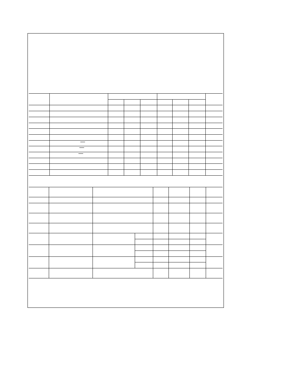
Recommended Operating Conditions
Symbol
Parameter
5497
DM7497
Units
Min
Nom
Max
Min
Nom
Max
V
CC
Supply Voltage
4 5
5
5 5
4 75
5
5 25
V
V
IH
High Level Input Voltage
2
2
V
V
IL
Low Level Input Voltage
0 8
0 8
V
I
OH
High Level Output Current
b
0 4
b
0 4
mA
I
OL
Low Level Output Current
16
16
mA
T
A
Free Air Operating Temperature
b
55
125
0
70
C
t
s
(L)
Setup Time LOW CE to CP Rising
25
25
ns
t
h
(H)
Hold Time HIGH CE to CP Rising
0
0
ns
t
h
(L)
Hold Time LOW CE to CP Falling
0
0
ns
t
w
(H)
CP Pulse Width HIGH
20
20
ns
t
w
(L)
CP Pulse Width LOW
20
ns
t
w
(H)
MR Pulse Width HIGH
15
15
ns
Electrical Characteristics
Over recommended operating free air temperature range (unless otherwise noted)
Symbol
Parameter
Conditions
Min
Typ
Max
Units
(Note 1)
V
I
Input Clamp Voltage
V
CC
e
Min I
I
e b
12 mA
b
1 5
V
V
OH
High Level Output
V
CC
e
Min I
OH
e
Max
2 4
3 4
V
Voltage
V
IL
e
Max
V
OL
Low Level Output
V
CC
e
Min I
OL
e
Max
0 2
0 4
V
Voltage
V
IH
e
Min
I
I
Input Current
Max
V
CC
e
Max V
I
e
5 5V
1
mA
Input Voltage
I
IH
High Level Input Current
V
CC
e
Max V
I
e
2 4V
DM74
40
m
A
Clock Inputs
54
80
I
IL
Low Level Input Current
V
CC
e
Max V
I
e
0 4V
DM74
b
1 6
mA
Clock Inputs
54
b
3 2
I
OS
Short Circuit
V
CC
e
Max
54
b
20
b
55
mA
Output Current
(Note 2)
DM74
b
18
b
55
I
CC
Supply Current With
V
CC
e
Max
120
mA
Outputs High
2
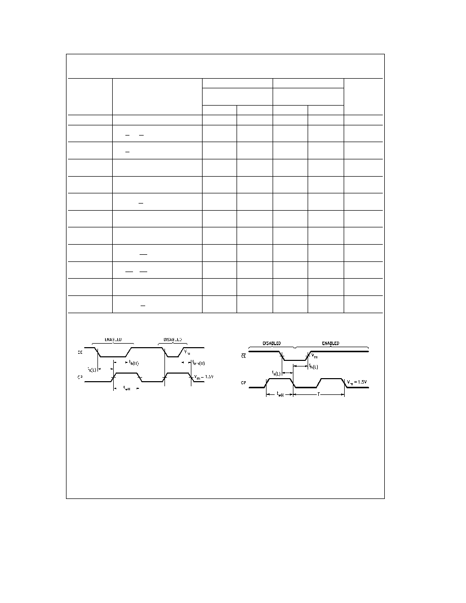
Switching Characteristics
V
CC
e a
5 0V T
A
e a
25 C (See Section 1 for waveforms and load configurations)
5497
DM7497
Symbol
Parameter
C
L
e
15 pF
C
L
e
15 pF
Units
R
L
e
400X
R
L
e
400X
Min
Max
Min
Max
f
max
Maximum Clock Frequency
25
25
MHz
t
PLH
Propagation Delay
18
18
ns
t
PHL
E
Z
to O
Z
23
23
t
PLH
Propagation Delay
30
30
ns
t
PHL
E
Z
to O
Y
33
33
t
PLH
Propagation Delay
14
14
ns
t
PHL
E
Y
to O
Y
10
10
t
PLH
Propagation Delay
23
23
ns
t
PHL
S
n
to O
Y
23
23
t
PLH
Propagation Delay
14
14
ns
t
PHL
S
n
to O
Z
14
14
t
PLH
Propagation Delay
39
39
ns
t
PHL
CP to O
Y
30
30
t
PLH
Propagation Delay
18
18
ns
t
PHL
CP to O
Z
26
26
t
PLH
Propagation Delay
35
30
ns
t
PHL
CP to TC
33
33
t
PLH
Propagation Delay
25
20
ns
t
PHL
CE to TC
21
21
t
PLH
Propagation Delay
43
36
ns
MR to O
Y
t
PHL
Propagation Delay
34
23
ns
MR to O
Z
Timing Diagrams
TL F 9780 ≠ 5
TL F 9780 ≠ 6
3
Functional Description
The '97 contains six JK flip-flops connected as a synchro-
nous modulo-64 binary counter A LOW signal on the Count
Enable (CE) input permits counting with all state changes
initiated simultaneously by the rising edge of the clock
When the count reaches maximum (63) with all Qs HIGH
the Terminal Count (TC) output will be LOW if CE is LOW A
HIGH signal on Master Reset (MR) resets the flip-flops and
prevents counting although output pulses can still occur if
the clock is running E
Z
is LOW and S5 is HIGH
The flip-flop outputs are decoded by a 6-wide AND-OR-IN-
VERT gate Each AND gate also contains the buffered and
inverted CP and Z-enable (E
Z
) functions as well as one of
the Select (S0 ≠ S5) inputs The Z output O
Z
is normally
HIGH and goes LOW when CP and E
Z
are LOW and any of
the AND gates has its other inputs HIGH The AND gates
are enabled by the counter at different times and different
rates relative to the clock For example the gate to which
S5 is connected is enabled during every other clock period
assuming S5 is HIGH Thus during one complete cycle of
the counter (64 clocks) the S5 gate is enabled 32 times and
can therefore gate 32 clocks per cycle to the output The S4
gate is enabled 16 times per cycle the S3 gate 8 times per
cycle etc The output pulse rate thus depends on the clock
rate and which of the S0 ≠ S5 inputs is HIGH
f
out
e
m
64
f
in
Where m
e
S5
2
5
a
S4
2
4
a
S3
2
3
a
S2
2
2
a
S1
2
1
a
S0
2
0
Thus by appropriate choice of signals applied to the S0 ≠ S5
inputs the output pulse rate can range from
to
of
the clock rate as suggested in Rate Select Table There is
no output pulse when the counter is in the ``all ones'' condi-
tion When m is 1 2 4 8 16 or 32 the output pulses are
evenly spaced assuming that the clock frequency is con-
stant For any other value of m the output pulses are not
evenly spaced since the pulse train is formed by interleav-
ing pulses passed by two or more of the AND gates The
Pulse Pattern Table indicates the output pattern for several
values of m In each row a one means that the O
Z
output
will be HIGH during that entire clock period while a zero
means that O
Z
will be LOW when the clock is LOW in that
period The first column in the output field coincides with the
``all zeroes'' condition of the counter while the last column
represents the ``all ones'' condition The pulse pattern for
any particular value of m can be deduced by factoring it into
the sum of appropriate powers of two (e g 19
e
16
a
2
a
1) and combining the pulses (i e
the zeroes) shown for
each for the relevant powers of two (e g for m
e
16 2 and
1)
The Y output O
Y
is the complement of O
Z
and is thus nor-
mally LOW A LOW signal on the Y-enable input E
Y
dis-
ables O
y
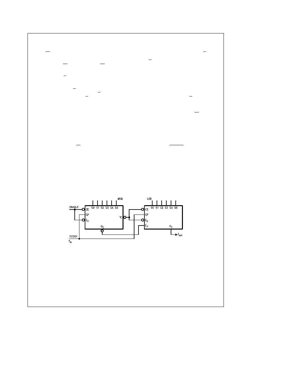
To expand the multiplier to 12-bit rate select two
packages can be cascaded as shown in
Figure A Both cir-
cuits operate from the basic clock with the TC output of the
first acting to enable both counting and the output pulses of
the second package Thus the second counter advances at
only
the rate of the first and a full cycle of the two coun-
ters combined requires 4096 clocks Each rate select input
of the first package has 64 times the weight of its counter-
part in the second package
f
out
e
m
1
a
m
2
64
64
f
in
Where m
1
e
S5
2
11
a
S4
2
10
a
S3
2
9
a
S2
2
8
a
S1
2
7
a
S0
2
6
(first package)
m
2
e
S5
2
5
a
S4
2
4
a
S3
2
3
a
S2
2
2
a
S1
2
1
a
S0
2
0
(second package)
Combined output pulses are obtained in
Figure A by letting
the Z output of the first circuit act as the Y-enable function
for the second with the interleaved pulses obtained from
the Y output of the second package being opposite in phase
to the clock
TL F 9780 ≠ 3
FIGURE A Cascading for 12-Bit Rate Select
4
Functional Description
(Continued)
Mode and Rate Select Table (Note 1)
Inputs
Clock
Outputs
Notes
MR
CE
E
Z
S5
S4
S3
S 2
S1
S0
Pulses
E
Y
O
Y
O
Z
TC
H
X
H
X
X
X
X
X
X
X
H
L
H
H
2
L
L
L
L
L
L
L
L
L
64
H
L
H
1
3
L
L
L
L
L
L
L
L
H
64
H
1
1
1
3
L
L
L
L
L
L
L
H
L
64
H
2
2
1
3
L
L
L
L
L
L
H
L
L
64
H
4
4
1
3
L
L
L
L
L
H
L
L
L
64
H
8
8
1
3
L
L
L
L
H
L
L
L
L
64
H
16
16
1
3
L
L
L
H
L
L
L
L
L
64
H
32
32
1
3
L
L
L
H
H
H
H
H
H
64
H
63
62
1
3
L
L
L
H
H
H
H
H
H
64
L
H
63
1
4
L
L
L
H
L
L
L
L
L
64
H
40
40
1
5
H
e
HIGH Voltage Level
L
e
LOW Voltage Level
X
e
Immaterial
Note 1
Numerals indicate number of pulses per cycle
Note 2
This is a simplified illustration of the clear function CP and E
Z
also affect the logic level of O
Y
and O
Z
A LOW signal on E
Y
will
cause O
Y
to remain HIGH
Note 3
Each rate illustrated assumes S0≠S5 are constant throughout the cycle however these illustrations in no way prohibit variable-
rate operation
Note 4
E
Y
is used to inhibit output Y
Note 5
f
out
e
m
f
in
64
e
(32
a
8) f
in
64
e
40 f
in
64
e
0 625 f
in
Pulse Pattern Table
m
Output Pulse Pattern at O
Z
1
1 1 1 1 1 1 1 1 1 1 1 1 1 1 1 1 1 1 1 1 1 1 1 1 1 1 1 1 1 1 1 0 1 1 1 1 1 1 1 1 1 1 1 1 1 1 1 1 1 1 1 1 1 1 1 1 1 1 1 1 1 1 1 1
2
1 1 1 1 1 1 1 1 1 1 1 1 1 1 1 0 1 1 1 1 1 1 1 1 1 1 1 1 1 1 1 1 1 1 1 1 1 1 1 1 1 1 1 1 1 1 1 0 1 1 1 1 1 1 1 1 1 1 1 1 1 1 1 1
3
1 1 1 1 1 1 1 1 1 1 1 1 1 1 1 0 1 1 1 1 1 1 1 1 1 1 1 1 1 1 1 0 1 1 1 1 1 1 1 1 1 1 1 1 1 1 1 0 1 1 1 1 1 1 1 1 1 1 1 1 1 1 1 1
4
1 1 1 1 1 1 1 0 1 1 1 1 1 1 1 1 1 1 1 1 1 1 1 0 1 1 1 1 1 1 1 1 1 1 1 1 1 1 1 0 1 1 1 1 1 1 1 1 1 1 1 1 1 1 1 0 1 1 1 1 1 1 1 1
5
1 1 1 1 1 1 1 0 1 1 1 1 1 1 1 1 1 1 1 1 1 1 1 0 1 1 1 1 1 1 1 0 1 1 1 1 1 1 1 0 1 1 1 1 1 1 1 1 1 1 1 1 1 1 1 0 1 1 1 1 1 1 1 1
6
1 1 1 1 1 1 1 0 1 1 1 1 1 1 1 0 1 1 1 1 1 1 1 0 1 1 1 1 1 1 1 1 1 1 1 1 1 1 1 0 1 1 1 1 1 1 1 0 1 1 1 1 1 1 1 0 1 1 1 1 1 1 1 1
8
1 1 1 0 1 1 1 1 1 1 1 0 1 1 1 1 1 1 1 0 1 1 1 1 1 1 1 0 1 1 1 1 1 1 1 0 1 1 1 1 1 1 1 0 1 1 1 1 1 1 1 0 1 1 1 1 1 1 1 0 1 1 1 1
1 0
1 1 1 0 1 1 1 1 1 1 1 0 1 1 1 1 1 1 1 0 1 1 1 1 1 1 1 0 1 1 1 1 1 1 1 0 1 1 1 1 1 1 1 0 1 1 1 0 1 1 1 0 1 1 1 1 1 1 1 0 1 1 1 1
12
1 1 1 0 1 1 1 0 1 1 1 0 1 1 1 1 1 1 1 0 1 1 1 0 1 1 1 0 1 1 1 1 1 1 1 0 1 1 1 0 1 1 1 0 1 1 1 1 1 1 1 0 1 1 1 0 1 1 1 0 1 1 1 1
14
1 1 1 0 1 1 1 0 1 1 1 0 1 1 1 0 1 1 1 0 1 1 1 0 1 1 1 0 1 1 1 1 1 1 1 0 1 1 1 0 1 1 1 0 1 1 1 0 1 1 1 0 1 1 1 0 1 1 1 0 1 1 1 1
16
1 0 1 1 1 0 1 1 1 0 1 1 1 0 1 1 1 0 1 1 1 0 1 1 1 0 1 1 1 0 1 1 1 0 1 1 1 0 1 1 1 0 1 1 1 0 1 1 1 0 1 1 1 0 1 1 1 0 1 1 1 0 1 1
20
1 0 1 1 1 0 1 0 1 0 1 1 1 0 1 1 1 0 1 1 1 0 1 0 1 0 1 1 1 0 1 1 1 0 1 1 1 0 1 0 1 0 1 1 1 0 1 1 1 0 1 1 1 0 1 1 1 0 1 1 1 0 1 1
24
1 0 1 0 1 0 1 1 1 0 1 0 1 0 1 1 1 0 1 0 1 0 1 1 1 0 1 0 1 0 1 1 1 0 1 0 1 0 1 1 1 1 1 0 1 0 1 1 1 0 1 0 1 0 1 1 1 0 1 0 1 0 1 1
28
1 0 1 0 1 0 1 0 1 0 1 0 1 0 1 1 1 0 1 0 1 0 1 0 1 0 1 0 1 0 1 1 1 0 1 0 1 0 1 0 1 0 1 0 1 0 1 1 1 0 1 0 1 0 1 0 1 0 1 0 1 0 1 1
32
0 1 0 1 0 1
0 1 0 1
5