
TL F 6271
DM64ALS08DM74ALS08
Quad
2-Input
AND
Gate
August 1995
DM64ALS08 DM74ALS08
Quad 2-Input AND Gate
General Description
This device contains four independent gates each of which
performs the logic AND function
The DM64ALS08 version features the same performance
as the standard version DM74ALS08 with a guarantee over
an extended temperature range (
b
40 C to
a
85 C)
Features
Y
Switching specifications at 50 pF
Y
Switching specifications guaranteed over full tempera-
ture and V
CC
range
Y
Advanced oxide-isolated
ion-implanted Schottky TTL
process
Y
Functionally and pin for pin compatible with Schottky
and low power Schottky TTL counterpart
Y
Improved AC performance over Schottky and low pow-
er Schottky counterparts
Y
DM64ALS08 guaranteed over extended temperature
b
40 C to
a
85 C
Connection Diagram
Dual-In-Line Package
TL F 6271 � 1
Order Number DM64ALS08M DM64ALS08N DM74ALS08M DM74ALS08N or DM74ALS08SJ
See NS Package Number M14A M14D or N14A
Function Table
Y
e
AB
Inputs
Output
A
B
Y
L
L
L
L
H
L
H
L
L
H
H
H
H
e
High Logic Level
L
e
Low Logic Level
C1995 National Semiconductor Corporation
RRD-B30M115 Printed in U S A

Absolute Maximum Ratings
Supply Voltage
7V
Input Voltage
7V
Operating Free Air Temperature Range
DM74ALS
0 C to
a
70 C
DM64ALS
b
40 C to
a
85 C
Storage Temperature Range
b
65 C to
a
150 C
Typical i
JA
N Package
89 C W
M Package
120 C W
Note
The ``Absolute Maximum Ratings'' are those values
beyond which the safety of the device cannot be guaran-
teed The device should not be operated at these limits The
parametric values defined in the ``Electrical Characteristics''
table are not guaranteed at the absolute maximum ratings
The ``Recommended Operating Conditions'' table will define
the conditions for actual device operation
Recommended Operating Conditions
Symbol
Parameter
DM64ALS08
DM74ALS08
Units
Min
Nom
Max
Min
Nom
Max
V
CC
Supply Voltage
4 5
5
5 5
4 5
5
5 5
V
V
IH
High Level Input Voltage
2
2
V
V
IL
Low Level Input Voltage
0 8
0 8
V
I
OH
High Level Output Current
b
0 4
b
0 4
mA
I
OL
Low Level Output Current
8
8
mA
T
A
Free Air Operating Temperature
b
40
85
0
70
C
Electrical Characteristics
over recommended operating free air temperature range All typical values are measured at V
CC
e
5V T
A
e
25 C
Symbol
Parameter
Conditions
Min
Typ
Max
Units
V
IK
Input Clamp Voltage
V
CC
e
4 5V I
I
e b
18 mA
b
1 5
V
V
OH
High Level Output
I
OH
e b
0 4 mA
V
CC
b
2
V
Voltage
V
CC
e
4 5V to 5 5V
V
OL
Low Level Output
V
CC
e
4 5V
I
OL
e
4 mA
0 25
0 4
V
Voltage
I
OL
e
8 mA
0 35
0 5
V
I
I
Input Current
Max
V
CC
e
5 5V V
IH
e
7V
0 1
mA
Input Voltage
I
IH
High Level Input Current
V
CC
e
5 5V V
IH
e
2 7V
20
m
A
I
IL
Low Level Input Current
V
CC
e
5 5V V
IL
e
0 4V
b
0 1
mA
I
O
Output Drive Current
V
CC
e
5 5V
V
O
e
2 25V
b
30
b
112
mA
I
CC
Supply Current
V
CC
e
5 5V
Outputs High
1 3
2 4
mA
Outputs Low
2 2
4
mA
Switching Characteristics
over recommended operating free air temperature range (Note 1)
Symbol
Parameter
Conditions
DM64ALS08
DM74ALS08
Units
Min
Max
Min
Max
t
PLH
Propagation Delay Time
V
CC
e
4 5V to 5 5V
4
14
4
14
ns
Low to High Level Output
R
L
e
500X
t
PHL
Propagation Delay Time
C
L
e
50 pF
3
10
3
10
ns
High to Low Level Output
Note 1
See Section 5 for test waveforms and output load
2
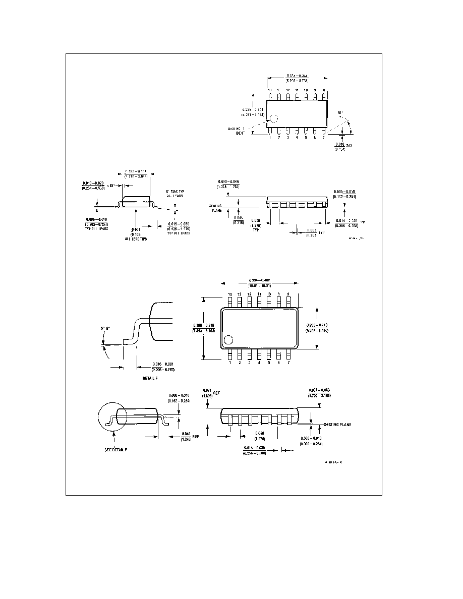
Physical Dimensions
inches (millimeters)
S O Package (M)
Order Number DM64ALS08M or DM74ALS08M
NS Package Number M14A
Small Outline Package (SJ)
Order Number DM74ALS08SJ
NS Package Number M14D
3
DM64ALS08DM74ALS08
Quad
2-Input
AND
Gate
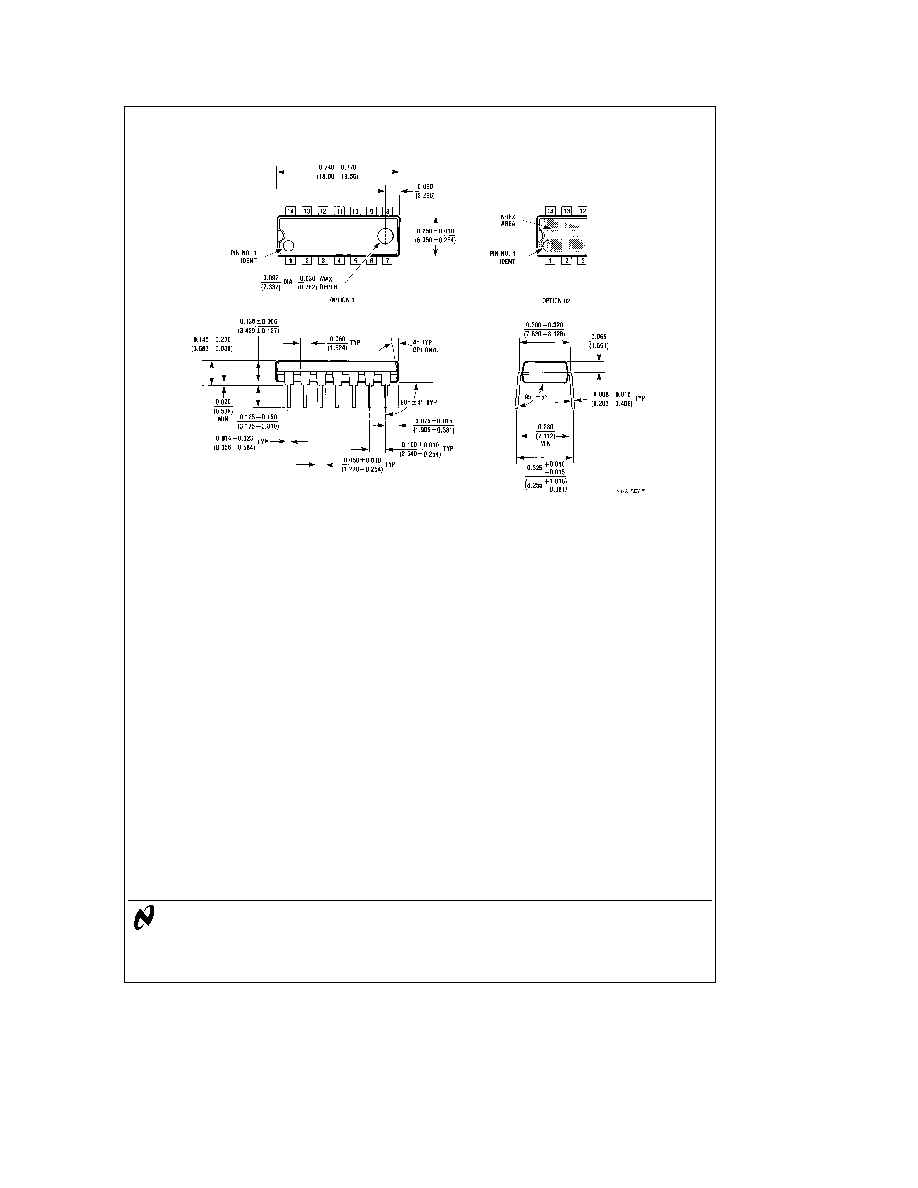
Physical Dimensions
inches (millimeters) (Continued)
Molded Dual-In-Line Package (N)
Order Number DM64ALS08N or DM74ALS08N
NS Package Number N14A
LIFE SUPPORT POLICY
NATIONAL'S PRODUCTS ARE NOT AUTHORIZED FOR USE AS CRITICAL COMPONENTS IN LIFE SUPPORT
DEVICES OR SYSTEMS WITHOUT THE EXPRESS WRITTEN APPROVAL OF THE PRESIDENT OF NATIONAL
SEMICONDUCTOR CORPORATION As used herein
1 Life support devices or systems are devices or
2 A critical component is any component of a life
systems which (a) are intended for surgical implant
support device or system whose failure to perform can
into the body or (b) support or sustain life and whose
be reasonably expected to cause the failure of the life
failure to perform when properly used in accordance
support device or system or to affect its safety or
with instructions for use provided in the labeling can
effectiveness
be reasonably expected to result in a significant injury
to the user
National Semiconductor
National Semiconductor
National Semiconductor
National Semiconductor
Corporation
Europe
Hong Kong Ltd
Japan Ltd
1111 West Bardin Road
Fax (a49) 0-180-530 85 86
13th Floor Straight Block
Tel 81-043-299-2309
Arlington TX 76017
Email cnjwge tevm2 nsc com
Ocean Centre 5 Canton Rd
Fax 81-043-299-2408
Tel 1(800) 272-9959
Deutsch Tel (a49) 0-180-530 85 85
Tsimshatsui Kowloon
Fax 1(800) 737-7018
English
Tel (a49) 0-180-532 78 32
Hong Kong
Fran ais Tel (a49) 0-180-532 93 58
Tel (852) 2737-1600
Italiano
Tel (a49) 0-180-534 16 80
Fax (852) 2736-9960
National does not assume any responsibility for use of any circuitry described no circuit patent licenses are implied and National reserves the right at any time without notice to change said circuitry and specifications