TL F 6220
DM74ALS373
Octal
D-Type
TRI-STATE
Transparent
Latch
March 1996
DM74ALS373
Octal D-Type TRI-STATE
Transparent Latch
General Description
These 8-bit registers feature totem-pole TRI-STATE outputs
designed specifically for driving highly-capacitive or relative-
ly low-impedance loads The high-impedance state and in-
creased high-logic-level drive provide these registers with
the capability of being connected directly to and driving the
bus lines in a bus-organized system without need for inter-
face or pull-up components They are particularly attractive
for implementing buffer registers I O ports bidirectional
bus drivers and working registers
The eight latches of the ALS373 are transparent D-type
latches While the enable (G) is high the Q outputs will fol-
low the data (D) inputs When the enable is taken low the
output will be latched at the level of the data that was set
up
A buffered output control input can be used to place the
eight outputs in either a normal logic state (high or low logic
levels) or a high-impedance state In the high-impedance
state the outputs neither load nor drive the bus lines signifi-
cantly
The output control does not affect the internal operation of
the latches That is the old data can be retained or new
data can be entered even while the outputs are off
Features
Y
Switching specifications at 50 pF
Y
Switching specifications guaranteed over full tempera-
ture and V
CC
range
Y
Advanced oxide-isolated
ion-implanted Schottky TTL
process
Y
Functionally and pin for pin compatible with LS TTL
counterpart
Y
Improved AC performance over LS373 at approximately
half the power
Y
TRI-STATE buffer-type outputs drive bus lines directly
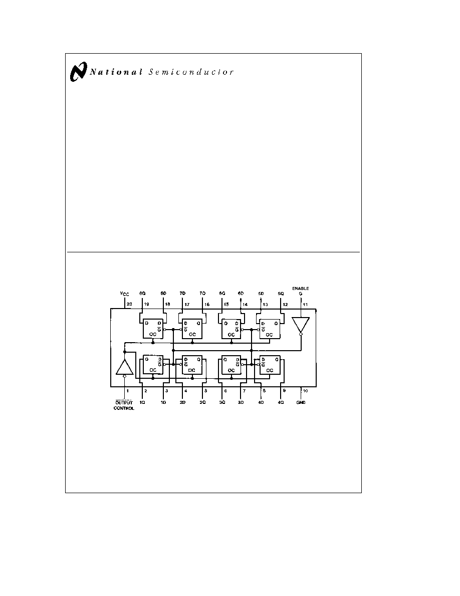
Connection Diagram
Dual-In-Line Package
TL F 6220 � 1
Order Number DM74ALS373WM DM74ALS373N or DM74ALS373SJ
See NS Package Number M20B M20D or N20A
TRI-STATE
is a registered trademark of National Semiconductor Corporation
C1996 National Semiconductor Corporation
RRD-B30M36 Printed in U S A
http
www national com
Absolute Maximum Ratings
Supply Voltage
7V
Input Voltage
7V
Voltage Applied to Disabled Output
5 5V
Operating Free Air Temperature Range
DM74ALS
0 C to
a
70 C
Storage Temperature Range
b
65 C to
a
150 C
Typical i
JA
N Package
57 0 C W
M Package
76 0 C W
Note
This product meets application requirements of 500 temperature cy-
cles from
b
65 C to
a
150 C
Note
The ``Absolute Maximum Ratings'' are those values
beyond which the safety of the device cannot be guaran-
teed The device should not be operated at these limits The
parametric values defined in the ``Electrical Characteristics''
table are not guaranteed at the absolute maximum ratings
The ``Recommended Operating Conditions'' table will define
the conditions for actual device operation
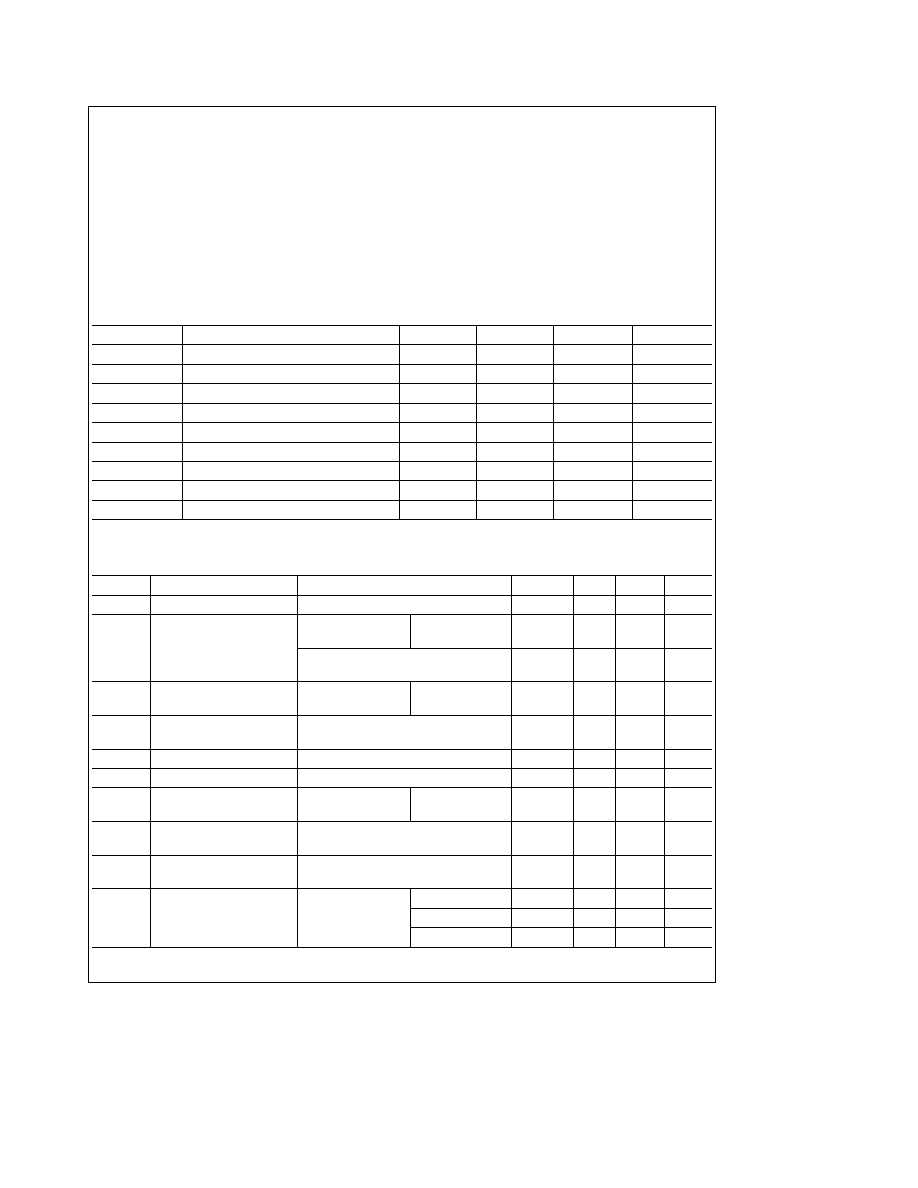
Recommended Operating Conditions
Symbol
Parameter
Min
Nom
Max
Units
V
CC
Supply Voltage
4 5
5
5 5
V
V
IH
High Level Input Voltage
2
V
V
IL
Low Level Input Voltage
0 8
V
I
OH
High Level Output Current
b
2 6
mA
I
OL
Low Level Output Current
24
mA
t
W
Width of Enable Pulse High or Low
10
ns
t
SU
Data Setup Time
10
v
ns
t
H
Data Hold Time
7
v
ns
T
A
Free Air Operating Temperature
0
70
C
The (
v
) arrow indicates the negative edge of the enable is used for reference
Electrical Characteristics
over recommended operating free air temperature range All typical values are measured at V
CC
e
5V T
A
e
25 C
Symbol
Parameter
Conditions
Min
Typ
Max
Units
V
IK
Input Clamp Voltage
V
CC
e
4 5V I
I
e b
18 mA
b
1 5
V
V
OH
High Level Output
V
CC
e
4 5V
I
OH
e b
2 6 mA
2 4
3 3
V
Voltage
V
CC
e
4 5V to 5 5V
V
CC
b
2
V
I
OH
e b
400 mA
V
OL
Low Level Output
V
CC
e
4 5V
I
OL
e
24 mA
0 35
0 5
V
Voltage
I
I
Input Current at Max
V
CC
e
5 5V V
IH
e
7V
0 1
mA
Input Voltage
I
IH
High Level Input Current
V
CC
e
5 5V V
IH
e
2 7V
20
m
A
I
IL
Low Level Input Current
V
CC
e
5 5V V
IL
e
0 4V
b
0 1
mA
I
O
Output Drive Current
V
CC
e
5 5V
V
O
e
2 25V
b
30
b
112
mA
I
OZH
Off-State Output Current
V
CC
e
5 5V
20
m
A
High Level Voltage Applied
V
O
e
2 7V
I
OZL
Off-State Output Current
V
CC
e
5 5V
b
20
m
A
Low Level Voltage Applied
V
O
e
0 4V
I
CC
Supply Current
V
CC
e
5 5V
Outputs High
9
16
mA
Outputs Open
Outputs Low
16
25
mA
Outputs Disabled
17
27
mA
http
www national com
2

Switching Characteristics
over recommended operating free air temperature range (Note 1)
Symbol
Parameter
Conditions
From
To
Min
Max
Units
t
PLH
Propagation Delay Time
V
CC
e
4 5V to 5 5V
Data
Any Q
2
12
ns
Low to High Level Output
R
L
e
500X
t
PHL
Propagation Delay Time
C
L
e
50 pF
Data
Any Q
4
16
ns
High to Low Level Output
t
PLH
Propagation Delay Time
Enable
Any Q
6
22
ns
Low to High Level Output
t
PHL
Propagation Delay Time
Enable
Any Q
7
23
ns
High to Low Level Output
t
PZH
Output Enable Time
Output
Any Q
6
18
ns
to High Level Output
Control
t
PZL
Output Enable Time
Output
Any Q
5
20
ns
to Low Level Output
Control
t
PHZ
Output Disable Time
Output
Any Q
2
10
ns
from High Level Output
Control
t
PLZ
Output Disable Time
Output
Any Q
2
12
ns
from Low Level Output
Control
Note 1
See Section 5 for test waveforms and output load
Function Table
Output
Enable
D
Output
Control
G
Q
L
H
H
H
L
H
L
L
L
L
X
Q
0
H
X
X
Z
L
e
Low State H
e
High State X
e
Don't Care
Z
e
High Impedance State
Q
0
e
Previous Condition of Q
http
www national com
3
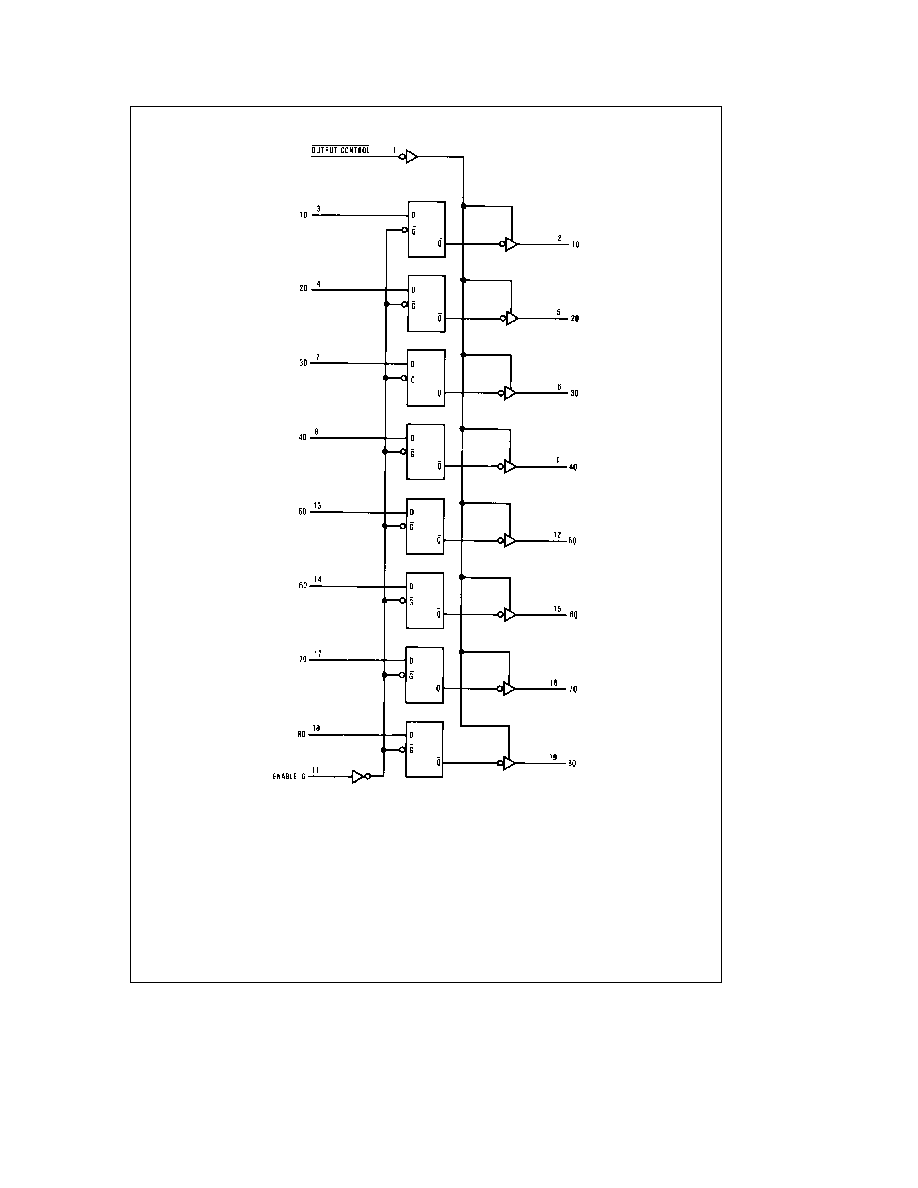
Logic Diagram
TL F 6220 � 2
http
www national com
4
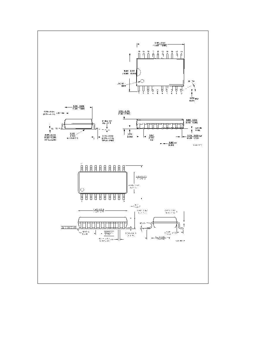
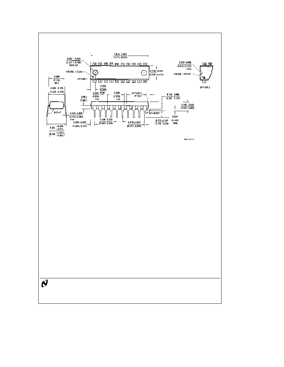
Physical Dimensions
inches (millimeters)
S O Package (M)
Order Number DM74ALS373WM
NS Package Number M20B
Small Outline Package (SJ)
Order Number DM74ALS373SJ
NS Package Number M20D
http
www national com
5
DM74ALS373
Octal
D-Type
TRI-STATE
Transparent
Latch
Physical Dimensions
inches (millimeters) (Continued)
Molded Dual-In-Line Package (N)
Order Number DM74ALS373N
NS Package Number N20A
LIFE SUPPORT POLICY
NATIONAL'S PRODUCTS ARE NOT AUTHORIZED FOR USE AS CRITICAL COMPONENTS IN LIFE SUPPORT
DEVICES OR SYSTEMS WITHOUT THE EXPRESS WRITTEN APPROVAL OF THE PRESIDENT OF NATIONAL
SEMICONDUCTOR CORPORATION As used herein
1 Life support devices or systems are devices or
2 A critical component is any component of a life
systems which (a) are intended for surgical implant
support device or system whose failure to perform can
into the body or (b) support or sustain life and whose
be reasonably expected to cause the failure of the life
failure to perform when properly used in accordance
support device or system or to affect its safety or
with instructions for use provided in the labeling can
effectiveness
be reasonably expected to result in a significant injury
to the user
National Semiconductor
National Semiconductor
National Semiconductor
National Semiconductor
Corporation
Europe
Hong Kong Ltd
Japan Ltd
1111 West Bardin Road
Fax a49 (0) 180-530 85 86
13th Floor Straight Block
Tel 81-043-299-2308
Arlington TX 76017
Email europe support nsc com
Ocean Centre 5 Canton Rd
Fax 81-043-299-2408
Tel 1(800) 272-9959
Deutsch Tel a49 (0) 180-530 85 85
Tsimshatsui Kowloon
Fax 1(800) 737-7018
English
Tel a49 (0) 180-532 78 32
Hong Kong
Fran ais Tel a49 (0) 180-532 93 58
Tel (852) 2737-1600
http
www national com
Italiano
Tel a49 (0) 180-534 16 80
Fax (852) 2736-9960
National does not assume any responsibility for use of any circuitry described no circuit patent licenses are implied and National reserves the right at any time without notice to change said circuitry and specifications