TL F 6394
DM54LS154DM74LS154
4-Line
to
16-Line
DecodersDemultiplexers
May 1989
DM54LS154 DM74LS154 4-Line to 16-Line
Decoders Demultiplexers
General Description
Each of these 4-line-to-16-line decoders utilizes TTL circuit-
ry to decode four binary-coded inputs into one of sixteen
mutually exclusive outputs when both the strobe inputs G1
and G2 are low The demultiplexing function is performed
by using the 4 input lines to address the output line passing
data from one of the strobe inputs with the other strobe
input low When either strobe input is high all outputs are
high These demultiplexers are ideally suited for implement-
ing high-performance memory decoders All inputs are buff-
ered and input clamping diodes are provided to minimize
transmission-line effects and thereby simplify system de-
sign
Features
Y
Decodes 4 binary-coded inputs into one of 16 mutually
exclusive outputs
Y
Performs the demultiplexing function by distributing data
from one input line to any one of 16 outputs
Y
Input clamping diodes simplify system design
Y
High fan-out low-impedance totem-pole outputs
Y
Typical propagation delay
3 levels of logic 23 ns
Strobe 19 ns
Y
Typical power dissipation 45 mW
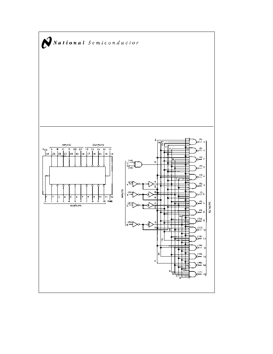
Connection and Logic Diagrams
Dual-In-Line Package
TL F 6394 � 1
Order Number DM54LS154J
DM74LS154WM or DM74LS154N
See NS Package Number J24A M24B or N24A
TL F 6394 � 2
C1995 National Semiconductor Corporation
RRD-B30M105 Printed in U S A
Absolute Maximum Ratings
(Note)
If Military Aerospace specified devices are required
please contact the National Semiconductor Sales
Office Distributors for availability and specifications
Supply Voltage
7V
Input Voltage
7V
Operating Free Air Temperature Range
DM54LS
b
55 C to
a
125 C
DM74LS
0 C to
a
70 C
Storage Temperature Range
b
65 C to
a
150 C
Note
The ``Absolute Maximum Ratings'' are those values
beyond which the safety of the device cannot be guaran-
teed The device should not be operated at these limits The
parametric values defined in the ``Electrical Characteristics''
table are not guaranteed at the absolute maximum ratings
The ``Recommended Operating Conditions'' table will define
the conditions for actual device operation
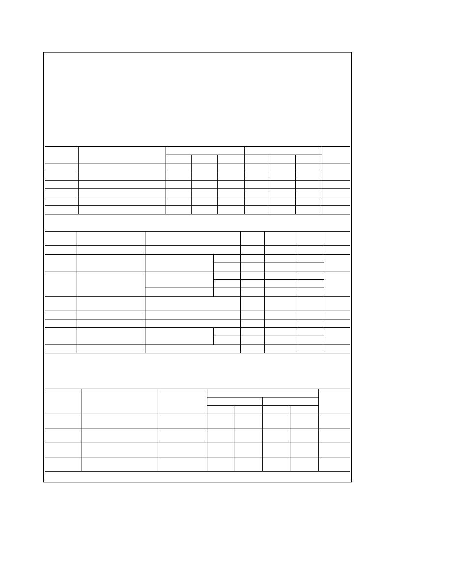
Recommended Operating Conditions
Symbol
Parameter
DM54LS154
DM74LS154
Units
Min
Nom
Max
Min
Nom
Max
V
CC
Supply Voltage
4 5
5
5 5
4 75
5
5 25
V
V
IH
High Level Input Voltage
2
2
V
V
IL
Low Level Input Voltage
0 7
0 8
V
I
OH
High Level Output Current
b
0 4
b
0 4
mA
I
OL
Low Level Output Current
4
8
mA
T
A
Free Air Operating Temperature
b
55
125
0
70
C
Electrical Characteristics
over recommended operating free air temperature range (unless otherwise noted)
Symbol
Parameter
Conditions
Min
Typ
Max
Units
(Note 1)
V
I
Input Clamp Voltage
V
CC
e
Min I
I
e b
18 mA
b
1 5
V
V
OH
High Level Output
V
CC
e
Min I
OH
e
Max
DM54
2 5
3 4
V
Voltage
V
IL
e
Max V
IH
e
Min
DM74
2 7
3 4
V
OL
Low Level Output
V
CC
e
Min I
OL
e
Max
DM54
0 25
0 4
Voltage
V
IL
e
Max V
IH
e
Min
DM74
0 35
0 5
V
I
OL
e
4 mA V
CC
e
Min
DM74
0 25
0 4
I
I
Input Current
Max
V
CC
e
Max V
I
e
7V
0 1
mA
Input Voltage
I
IH
High Level Input Current
V
CC
e
Max V
I
e
2 7V
20
m
A
I
IL
Low Level Input Current
V
CC
e
Max V
I
e
0 4V
b
0 4
mA
I
OS
Short Circuit
V
CC
e
Max
DM54
b
20
b
100
mA
Output Current
(Note 2)
DM74
b
20
b
100
I
CC
Supply Current
V
CC
e
Max (Note 3)
9
14
mA
Note 1
All typicals are at V
CC
e
5V T
A
e
25 C
Note 2
Not more than one output should be shorted at a time and the duration should not exceed one second
Note 3
I
CC
is measured with all outputs open and all inputs grounded
Switching Characteristics
at V
CC
e
5V and T
A
e
25 C (See Section 1 for Test Waveforms and Output Load)
From (Input)
R
L
e
2 kX
Symbol
Parameter
To (Output)
C
L
e
15 pF
C
L
e
50 pF
Units
Min
Max
Min
Max
t
PLH
Propagation Delay Time
Data to
30
35
ns
Low to High Level Output
Output
t
PHL
Propagation Delay Time
Data to
30
35
ns
High to Low Level Output
Output
t
PLH
Propagation Delay Time
Strobe to
20
25
ns
Low to High Level Output
Output
t
PHL
Propagation Delay Time
Strobe to
25
35
ns
High to Low Level Output
Output
2
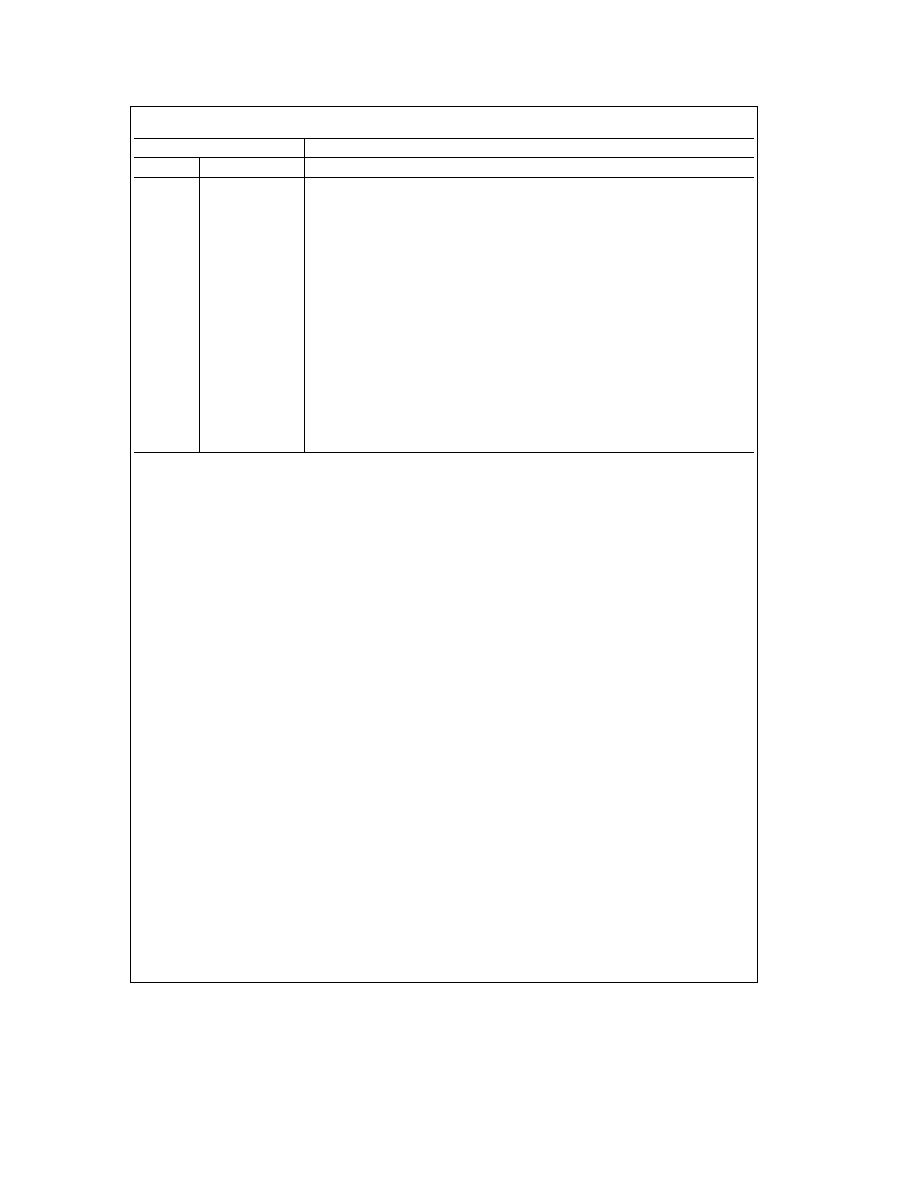
Function Table
Inputs
Outputs
G1
G2
D
C
B
A
0
1
2
3
4
5
6
7
8
9
10
11
12
13
14
15
L
L
L
L
L
L
L
H
H
H
H
H
H
H
H
H
H
H
H
H
H
H
L
L
L
L
L
H
H
L
H
H
H
H
H
H
H
H
H
H
H
H
H
H
L
L
L
L
H
L
H
H
L
H
H
H
H
H
H
H
H
H
H
H
H
H
L
L
L
L
H
H
H
H
H
L
H
H
H
H
H
H
H
H
H
H
H
H
L
L
L
H
L
L
H
H
H
H
L
H
H
H
H
H
H
H
H
H
H
H
L
L
L
H
L
H
H
H
H
H
H
L
H
H
H
H
H
H
H
H
H
H
L
L
L
H
H
L
H
H
H
H
H
H
L
H
H
H
H
H
H
H
H
H
L
L
L
H
H
H
H
H
H
H
H
H
H
L
H
H
H
H
H
H
H
H
L
L
H
L
L
L
H
H
H
H
H
H
H
H
L
H
H
H
H
H
H
H
L
L
H
L
L
H
H
H
H
H
H
H
H
H
H
L
H
H
H
H
H
H
L
L
H
L
H
L
H
H
H
H
H
H
H
H
H
H
L
H
H
H
H
H
L
L
H
L
H
H
H
H
H
H
H
H
H
H
H
H
H
L
H
H
H
H
L
L
H
H
L
L
H
H
H
H
H
H
H
H
H
H
H
H
L
H
H
H
L
L
H
H
L
H
H
H
H
H
H
H
H
H
H
H
H
H
H
L
H
H
L
L
H
H
H
L
H
H
H
H
H
H
H
H
H
H
H
H
H
H
L
H
L
L
H
H
H
H
H
H
H
H
H
H
H
H
H
H
H
H
H
H
H
L
L
H
X
X
X
X
H
H
H
H
H
H
H
H
H
H
H
H
H
H
H
H
H
L
X
X
X
X
H
H
H
H
H
H
H
H
H
H
H
H
H
H
H
H
H
H
X
X
X
X
H
H
H
H
H
H
H
H
H
H
H
H
H
H
H
H
H
e
High Level L
e
Low Level X
e
Don't Care
3

4
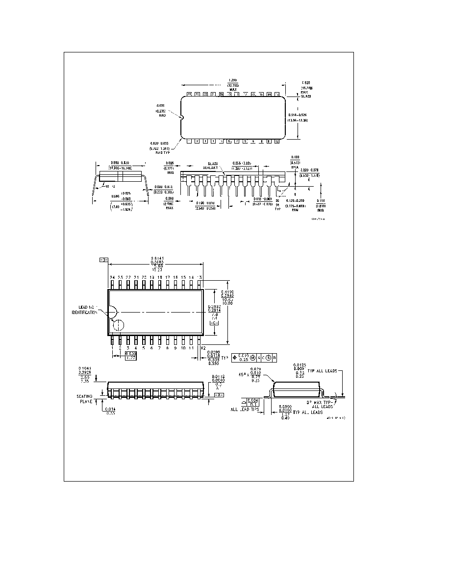
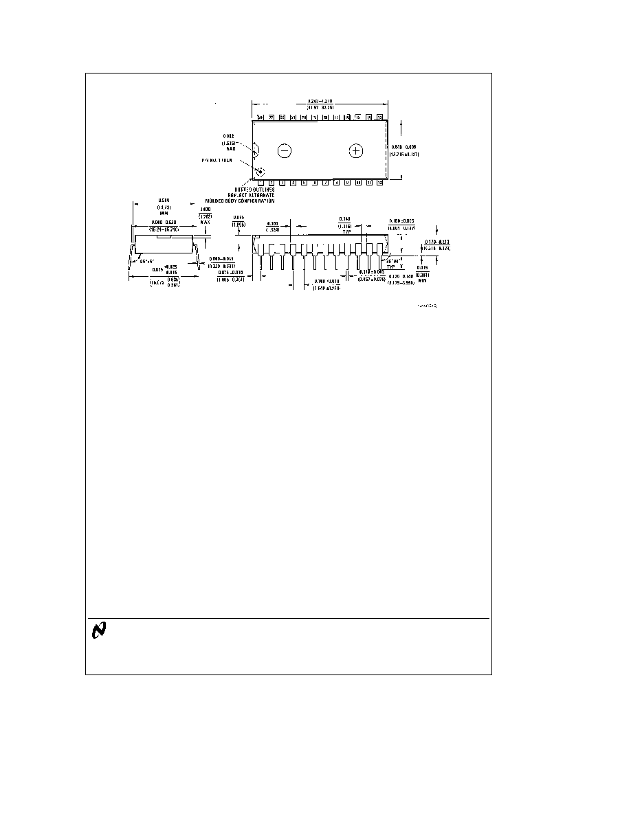
Physical Dimensions
inches (millimeters)
24-Lead Ceramic Dual-In-Line Package (J)
Order Number DM54LS154J
NS Package Number J24A
24-Lead Wide Small Outline Molded Package (M)
Order Number DM74LS154WM
NS Package Number M24B
5
DM54LS154DM74LS154
4-Line
to
16-Line
DecodersDemultiplexers
Physical Dimensions
inches (millimeters) (Continued)
24-Lead Molded Dual-In-Line Package (N)
Order Number DM74LS154N
NS Package Number N24A
LIFE SUPPORT POLICY
NATIONAL'S PRODUCTS ARE NOT AUTHORIZED FOR USE AS CRITICAL COMPONENTS IN LIFE SUPPORT
DEVICES OR SYSTEMS WITHOUT THE EXPRESS WRITTEN APPROVAL OF THE PRESIDENT OF NATIONAL
SEMICONDUCTOR CORPORATION As used herein
1 Life support devices or systems are devices or
2 A critical component is any component of a life
systems which (a) are intended for surgical implant
support device or system whose failure to perform can
into the body or (b) support or sustain life and whose
be reasonably expected to cause the failure of the life
failure to perform when properly used in accordance
support device or system or to affect its safety or
with instructions for use provided in the labeling can
effectiveness
be reasonably expected to result in a significant injury
to the user
National Semiconductor
National Semiconductor
National Semiconductor
National Semiconductor
Corporation
Europe
Hong Kong Ltd
Japan Ltd
1111 West Bardin Road
Fax (a49) 0-180-530 85 86
13th Floor Straight Block
Tel 81-043-299-2309
Arlington TX 76017
Email cnjwge tevm2 nsc com
Ocean Centre 5 Canton Rd
Fax 81-043-299-2408
Tel 1(800) 272-9959
Deutsch Tel (a49) 0-180-530 85 85
Tsimshatsui Kowloon
Fax 1(800) 737-7018
English
Tel (a49) 0-180-532 78 32
Hong Kong
Fran ais Tel (a49) 0-180-532 93 58
Tel (852) 2737-1600
Italiano
Tel (a49) 0-180-534 16 80
Fax (852) 2736-9960
National does not assume any responsibility for use of any circuitry described no circuit patent licenses are implied and National reserves the right at any time without notice to change said circuitry and specifications