 | –≠–ª–µ–∫—Ç—Ä–æ–Ω–Ω—ã–π –∫–æ–º–ø–æ–Ω–µ–Ω—Ç: DM74LS122 | –°–∫–∞—á–∞—Ç—å:  PDF PDF  ZIP ZIP |
TL F 6385
DM74LS122
Retriggerable
One-Shot
with
Clear
and
Complementary
Outputs
May 1989
DM74LS122 Retriggerable One-Shot with
Clear and Complementary Outputs
General Description
The DM74LS122 is a retriggerable monostable multivibrator
featuring both positive and negative edge triggering with
complementary outputs An internal 10 kX timing resistor is
provided for design convenience minimizing component
count and layout problems This device can be used with a
single external capacitor The 'LS122 has two active-low
transition triggering inputs (A) two active-high transition trig-
gering inputs (B) and a CLEAR input that terminates the
output pulse width at a predetermined time independent of
the timing components The clear (CLR) input also serves
as a trigger input when it is pulsed with a low level pulse
transition (
) To obtain optimum and trouble free opera-
tion please read operating rules and NSC one-shot applica-
tion notes carefully and observe recommendations
Features
Y
DC triggered from active-high transition or active-low
transition inputs
Y
Retriggerable to 100% duty cycle
Y
Over-riding clear terminates output pulse
Y
Internal 10 kX timing resistor
Y
TTL DTL compatible
Y
Compensated for V
CC
and temperature variations
Y
Input clamp diodes
Functional Description
The basic output pulse width is determined by selection of
the internal resistor R
INT
or an external resistor (R
X
) and
capacitor (C
X
) Once triggered the output pulse width may
be extended by retriggering the gated active-low (A) tran-
sition inputs or the active-high transition (B) inputs or the
CLEAR input The output pulse width can be reduced or
terminated by overriding it with the active-low CLEAR input
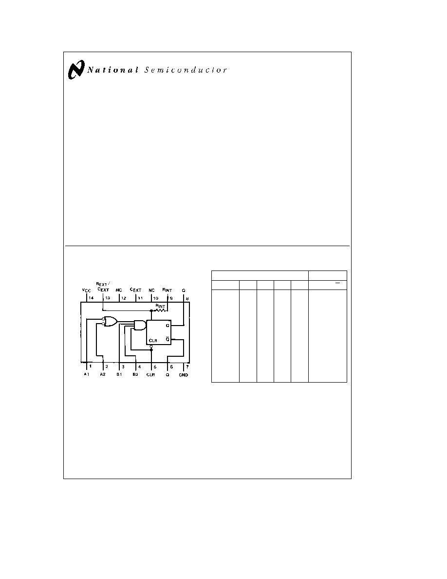
Connection Diagram
Dual-In-Line Package
TL F 6385 ≠ 1
Order Number DM74LS122M or DM74LS122N
See NS Package Number M14A or N14A
Function Table
Inputs
Outputs
CLEAR
A1
A2
B1
B2
Q
Q
L
X
X
X
X
L
H
X
H
H
X
X
L
H
X
X
X
L
X
L
H
X
X
X
X
L
L
H
H
L
X
u
H
H
L
X
H
u
H
X
L
u
H
H
X
L
H
u
H
H
v
H
H
H
v
v
H
H
H
v
H
H
H
u
L
X
H
H
u
X
L
H
H
H
e
High Logic Level
L
e
Low Logic Level
X
e
Can Be Either Low or High
u
e
Positive Going Transition
v
e
Negative Going Transition
e
A Positive Pulse
e
A Negative Pulse
C1995 National Semiconductor Corporation
RRD-B30M105 Printed in U S A
Absolute Maximum Ratings
(Note)
If Military Aerospace specified devices are required
please contact the National Semiconductor Sales
Office Distributors for availability and specifications
Supply Voltage
7V
Input Voltage
7V
Operating Free Air Temperature Range
DM74LS
0 C to
a
70 C
Storage Temperature
b
65 C to
a
150 C
Note
The ``Absolute Maximum Ratings'' are those values
beyond which the safety of the device cannot be guaran-
teed The device should not be operated at these limits The
parametric values defined in the ``Electrical Characteristics''
table are not guaranteed at the absolute maximum ratings
The ``Recommended Operating Conditions'' table will define
the conditions for actual device operation
Recommended Operating Conditions
Symbol
Parameters
Min
Nom
Max
Units
V
CC
Supply Voltage
4 75
5
5 25
V
V
IH
High Level Input Voltage
2
V
V
IL
Low Level Input Voltage
0 8
V
I
OH
High Level Output Current
b
0 4
mA
I
OL
Low Level Output Current
8
mA
t
W
Pulse Width
A or B High
40
(Note 6)
A or B Low
40
ns
Clear Low
40
R
EXT
External Timing Resistor
5
260
kX
C
EXT
External Timing Capacitance
No Restriction
m
F
C
WIRE
Wiring Capacitance
50
pF
at R
EXT
C
EXT
Terminal
T
A
Free Air Operating Temperature
0
70
C
Electrical Characteristics
over recommended operating free air temperature range (unless otherwise noted)
Symbol
Parameter
Conditions
Min
Typ
Max
Units
(Note 1)
V
I
Input Clamp Voltage
V
CC
e
Min I
e b
18 mA
b
1 5
V
V
OH
High Level Output
V
CC
e
Min I
OH
e
Max
2 7
3 4
V
Voltage
V
IL
e
Max V
IH
e
Min
V
OL
Low Level Output
V
CC
e
Min I
OL
e
Max
0 35
0 5
Voltage
V
IL
e
Max V
IH
e
Min
V
I
OL
e
4 mA V
CC
e
Min
0 25
0 4
I
I
Input Current
Max
V
CC
e
Max V
I
e
7V
0 1
mA
Input Voltage
I
IH
High Level Input Current
V
CC
e
Max V
I
e
2 7V
20
m
A
I
IL
Low Level Input Current
V
CC
e
Max V
I
e
0 4V
b
0 4
mA
I
OS
Short Circuit
V
CC
e
Max
b
20
b
100
mA
Output Current
(Note 2)
I
CC
Supply Current
V
CC
e
Max (Notes 3 4 and 5)
6
11
mA
2
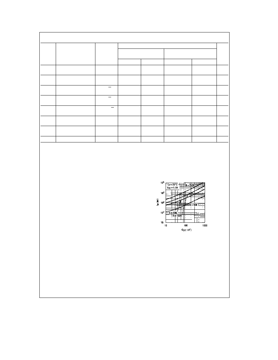
Switching Characteristics
at V
CC
e
5V and T
A
e
25 C (See Section 1 for Test Waveforms and Output Load)
R
L
e
2 kX
Symbol
Parameter
From (Input)
C
L
e
15 pF
C
L
e
15 pF
Units
To (Output)
C
EXT
e
0 pF R
EXT
e
5 kX
C
EXT
e
1000 pF R
EXT
e
10 kX
Min
Max
Min
Max
t
PLH
Propagation Delay Time
A to Q
33
ns
Low to High Level Output
t
PLH
Propagation Delay Time
B to Q
44
ns
Low to High Level Output
t
PHL
Propagation Delay Time
A to Q
45
ns
High to Low Level Output
t
PHL
Propagation Delay Time
B to Q
56
ns
High to Low Level Output
t
PLH
Propagation Delay Time
Clear to Q
45
ns
Low to High Level Output
t
PHL
Propagation Delay Time
Clear to Q
27
ns
High to Low Level Output
t
WQ(Min)
Minimum Width of Pulse
A or B to Q
200
ns
at Output Q
t
W(out)
Output Pulse Width
A or B to Q
4
5
m
s
Note 1
All typicals are at V
CC
e
5V T
A
e
25 C
Note 2
Not more than one output should be shorted at a time and the duration should not exceed one second
Note 3
Quiescent I
CC
is measured (after clearing) with 2 4V applied to all clear and A inputs B inputs grounded all outputs open C
EXT
e
0 02 mF and R
EXT
e
25 kX
Note 4
I
CC
is measured in the triggered state with 2 4V applied to all clear and B inputs A inputs grounded all outputs open C
EXT
e
0 02 mF and R
EXT
e
25 kX
Note 5
With all outputs open and 4 5V applied to all data and clear inputs I
CC
is measured after a momentary ground then 4 5V is applied to the clock
Note 6
T
A
e
25 C and V
CC
e
5V
Operating Rules
1 To use the internal 10 kX timing resistor connect the
R
INT
pin to V
CC
2 An external resistor (R
X
) or the internal resistor (10 kX)
and an external capacitor (C
X
) are required for proper
operation The value of C
X
may vary from 0 to any neces-
sary value For small time constants use high-quality
mica glass polypropylene polycarbonate or polystyrene
capacitors For large time constants use solid tantalum or
special aluminum capacitors If the timing capacitors
have leakages approaching 100 nA or if stray capaci-
tance from either terminal to ground is greater than 50 pF
the timing equations may not represent the pulse width
the device generates
3 The pulse width is essentially determined by external tim-
ing components R
X
and C
X
For C
X
k
1000 pF see
Fig-
ure 1 design curves on T
W
as function of timing compo-
nents value For C
X
l l
1000 pF the output is defined as
T
W
e
KR
X
C
X
where R
X
is in kX
C
X
is in pF
T
W
is in ns
K
0 37
TL F 6385 ≠ 2
FIGURE 1
3
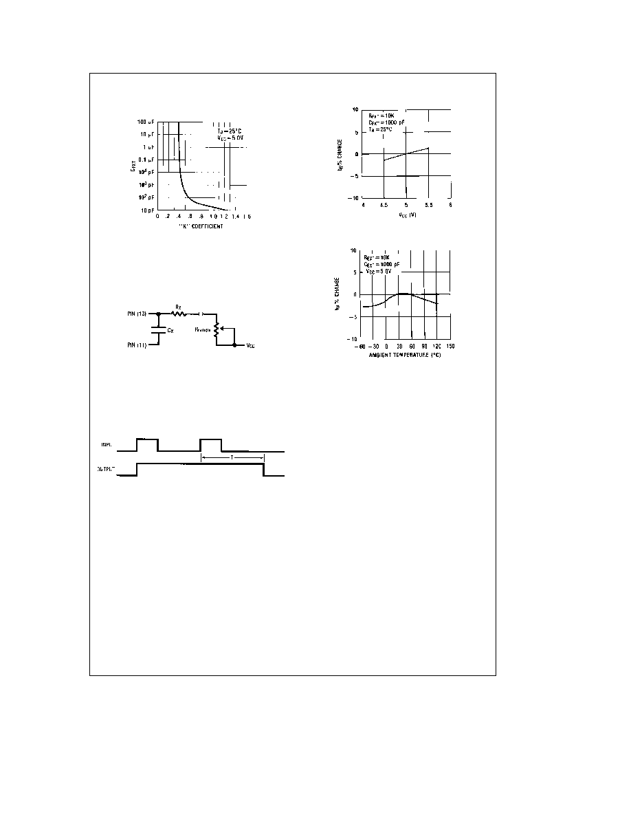
Operating Rules
(Continued)
The K factor is not a constant but varies with C
X
See
Figure 2
TL F 6385 ≠ 3
FIGURE 2
4 The switching diode required for most TTL one-shots
when using an electrolytic timing capacitor is not needed
for the 'LS122 and should not be used
5 To obtain variable pulse width by remote trimming the
following circuit is recommended
TL F 6385 ≠ 4
Note
``R
remote
'' should be as close to the device pins as possible
FIGURE 3
6 The retriggerable pulse width is calculated as shown be-
low
T
e
T
W
a
t
PLH
e
0 50
c
R
X
c
C
X
a
T
PLH
The retriggered pulse width is equal to the pulse width
plus a delay time period
(Figure 4)
TL F 6385 ≠ 5
FIGURE 4
7 Output pulse width variation versus V
CC
and operation
temperatures
Figure 5 depicts the relationship between
pulse width variation versus V
CC
and
Figure 6 depicts
pulse width variation versus temperatures
TL F 6385 ≠ 6
FIGURE 5
TL F 6385 ≠ 7
FIGURE 6
8 Under any operating condition C
X
and R
X
must be kept
as close to the one-shot device pins as possible to mini-
mize stray capacitance to reduce noise pick-up and to
reduce I-R and Ldi dt voltage developed along their con-
necting paths If the lead length from C
X
to pins (13) and
(11) is greater than 3 cm for example the output pulse
width might be quite different from values predicted from
the appropriate equations A non-inductive and low ca-
pacitive path is necessary to ensure complete discharge
of C
X
in each cycle of its operation so that the output
pulse width will be accurate
9 V
CC
and ground wiring should conform to good high-fre-
quency standards and practices so that switching tran-
sients on the V
CC
and ground return leads do not cause
interaction between one-shots A 0 01 mF to 0 10 mF by-
pass capacitor (disk ceramic or monolithic type) from V
CC
to ground is necessary on each device Furthermore the
bypass capacitor should be located as close to the V
CC
pin as space permits
For further detailed device characteristics and output performance
please refer to the NSC one-shot application note AN-366
4
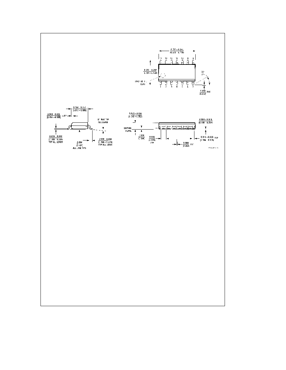
Physical Dimensions
inches (millimeters)
14-Lead Small Outline Molded Package (M)
Order Number DM74LS122M
NS Package Number M14A
5