TL F 10177
54LS160ADM74LS160A
54LS162ADM74LS162A
Synchronous
Presettable
BCD
Decade
Counters
May 1992
54LS160A DM74LS160A 54LS162A DM74LS162A
Synchronous Presettable BCD Decade Counters
General Description
The 'LS160 and 'LS162 are high speed synchronous dec-
ade counters operating in the BCD (8421) sequence They
are synchronously presettable for application in programma-
ble dividers and have two types of Count Enable inputs plus
a Terminal Count output for versatility in forming synchro-
nous multistage counters The 'LS160 has an asynchronous
Master Reset input that overrides all other inputs and forces
the outputs LOW The 'LS162 has a Synchronous Reset
input that overrides counting and parallel loading and allows
all outputs to be simultaneously reset on the rising edge of
the clock
Features
Y
Synchronous counting and loading
Y
High speed synchronous expansion
Y
Typical count rate of 35 MHz
Y
Fully edge triggered
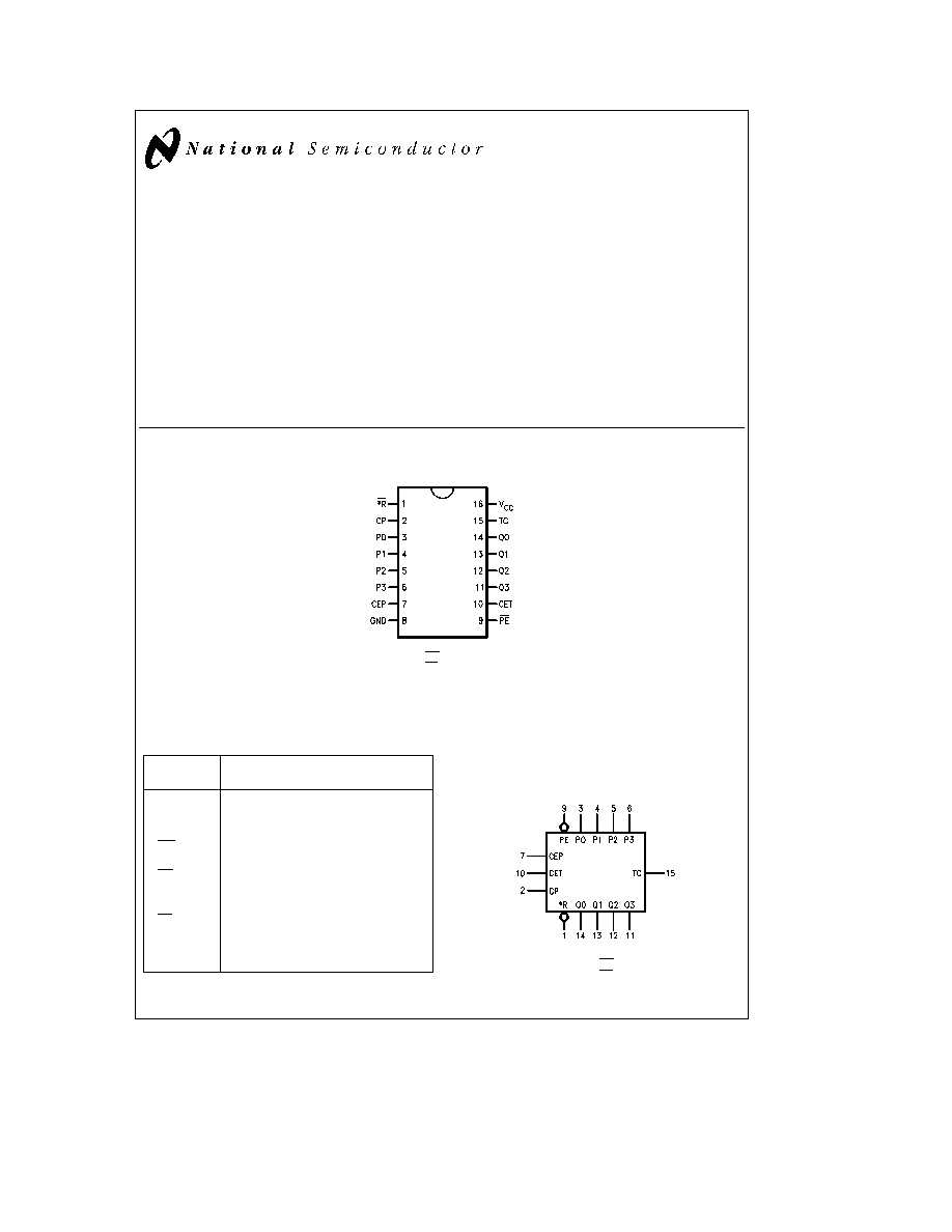
Connection Diagram
Dual-In-Line Package
TL F 10177 ≠ 1
MR for 'LS160
SR for 'LS162
Order Number 54LS160ADMQB 54LS160AFMQB 54LS160ALMQB
54LS162ADMQB 54LS162AFMQB 54LS162ALMQB DM74LS160AM
DM74LS160AN DM74LS162AM or DM74LS162AN
See NS Package Number E20A J16A M16A N16E or W16A
Pin
Description
Names
CEP
Count Enable Parallel Input
CET
Count Enable Trickle Input
CP
Clock Pulse Input (Active Rising Edge)
MR ('160)
Asynchronous Master Reset
Input (Active LOW)
SR ('162)
Synchronous Reset
Input (Active LOW)
P0 ≠ P3
Parallel Data Inputs
PE
Parallel Enable Input
(Active LOW)
Q0 ≠ Q3
Flip-Flop Outputs
TC
Terminal Count Output
Logic Symbol
TL F 10177 ≠ 2
V
CC
e
Pin 16
MR for 'LS160
GND
e
Pin 8
SR for 'LS162
C1995 National Semiconductor Corporation
RRD-B30M105 Printed in U S A
Absolute Maximum Ratings
(Note)
If Military Aerospace specified devices are required
please contact the National Semiconductor Sales
Office Distributors for availability and specifications
Supply Voltage
7V
Input Voltage
7V
Operating Free Air Temperature Range
54LS
b
55 C to
a
125 C
DM74LS
0 C to
a
70 C
Storage Temperature Range
b
65 C to
a
150 C
Note
The ``Absolute Maximum Ratings'' are those values
beyond which the safety of the device cannot be guaran-
teed The device should not be operated at these limits The
parametric values defined in the ``Electrical Characteristics''
table are not guaranteed at the absolute maximum ratings
The ``Recommended Operating Conditions'' table will define
the conditions for actual device operation
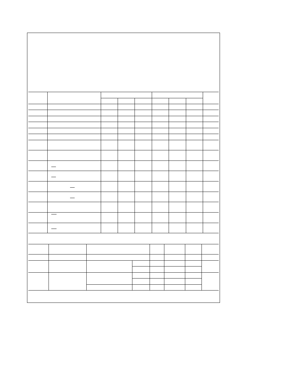
Recommended Operating Conditions
Symbol
Parameter
54LS160A 162A
DM74LS160A 162A
Units
Min
Nom
Max
Min
Nom
Max
V
CC
Supply Voltage
4 5
5
5 5
4 75
5
5 25
V
V
IH
High Level Input Voltage
2
2
V
V
IL
Low Level Input Voltage
0 7
0 8
V
I
OH
High Level Output Current
b
0 4
b
0 4
mA
I
OL
Low Level Output Current
4
8
mA
T
A
Free Air Operating Temperature
b
55
125
0
70
C
t
s
(H)
Setup Time HIGH or LOW
20
20
ns
t
s
(L)
P
n
to CP
20
20
t
h
(H)
Hold Time HIGH or LOW
0 0
0 0
ns
t
h
(L)
P
n
to CP
0 0
0 0
t
s
(H)
Setup Time HIGH or LOW
20
20
ns
t
s
(L)
PE to CP
20
20
t
h
(H)
Hold Time HIGH or LOW
0
0
ns
t
h
(L)
PE to CP
0
0
t
s
(H)
Setup Time HIGH or LOW
20
20
ns
t
s
(L)
CEP CET or SR to CP
20
20
t
h
(H)
Hold Time HIGH or LOW
0
0
ns
t
h
(L)
CEP CET or SR to CP
0
0
t
w
(H)
CP Pulse Width
15
15
ns
t
w
(L)
HIGH or LOW
25
25
t
w
(L)
MR Pulse Width
15
15
ns
LOW ('160)
t
rec
Recovery Time
20
20
ns
MR to CP ('160)
Electrical Characteristics
over recommended operating free air temperature range (unless otherwise noted)
Symbol
Parameter
Conditions
Min
Typ
Max
Units
(Note 1)
V
I
Input Clamp Voltage
V
CC
e
Min I
I
e b
18 mA
b
1 5
V
V
OH
High Level Output
V
CC
e
Min I
OH
e
Max
54LS
2 5
V
Voltage
V
IL
e
Max
DM74
2 7
V
OL
Low Level Output
V
CC
e
Min I
OL
e
Max
54LS
0 4
Voltage
V
IH
e
Min
DM74
0 5
V
I
OL
e
4 mA V
CC
e
Min
DM74
0 4
Note 1
All typicals are at V
CC
e
5V T
A
e
25 C
Note 2
Not more than one output should be shorted at a time and the duration should not exceed one second
2
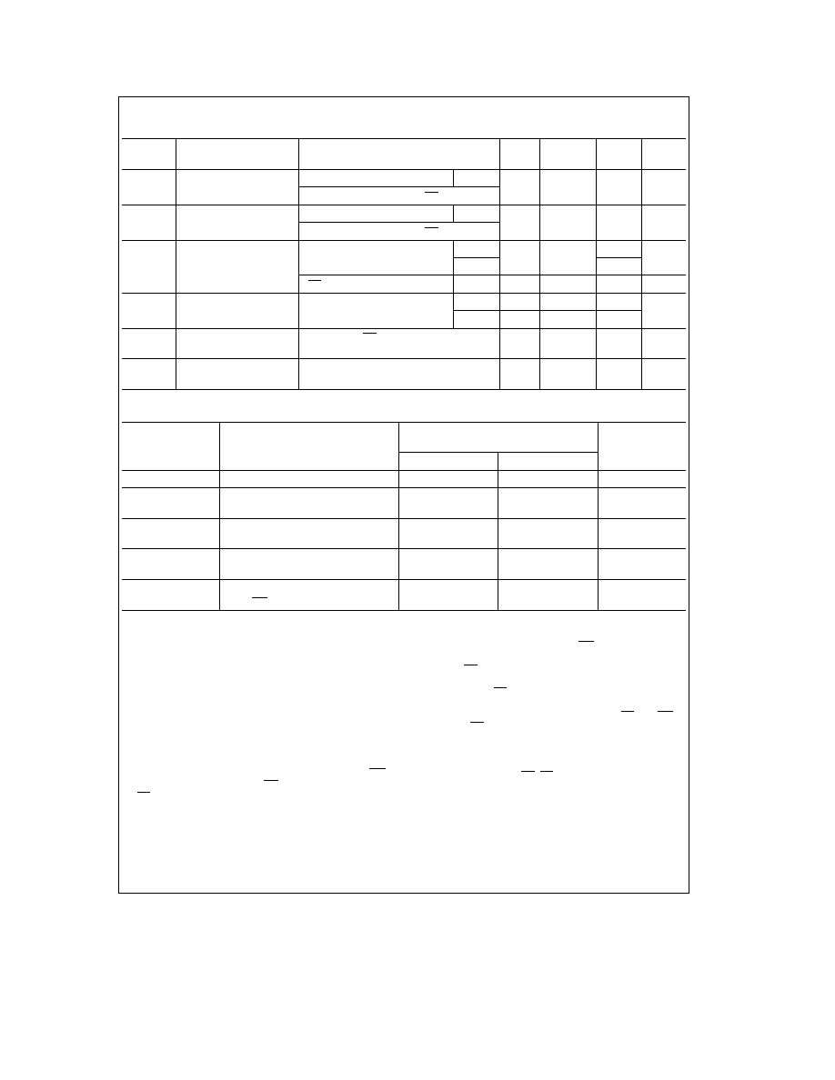
Electrical Characteristics
over recommended operating free air temperature range (unless otherwise noted) (Continued)
Symbol
Parameter
Conditions
Min
Typ
Max
Units
(Note 1)
I
I
Input Current
Max
V
CC
e
Max V
I
e
7V
Other
0 1
mA
Input Voltage
PE CET Inputs
0 2
I
IH
High Level Input Current
V
CC
e
Max V
I
e
2 7V
Other
20
m
A
PE CET Inputs
40
I
IL
Low Level Input Current
V
CC
e
Max V
I
e
0 4V Inputs
54LS
b
0 4
mA
DM74
b
1 6
PE CET Inputs
b
0 8
mA
I
OS
Short Circuit
V
CC
e
Max
54LS
b
20
b
100
mA
Output Current
(Note 2)
DM74
b
20
b
100
I
CCH
Supply Current with
V
CC
e
Max PE
e
GND
31
mA
Outputs HIGH
CP
e
L Other Inputs
e
4 5V
I
CCL
Supply Current with
V
CC
e
Max V
IN
e
GND
31
mA
Outputs LOW
CP
e
L
Switching Characteristics
V
CC
e a
5 0V T
A
e a
25 C
R
L
e
2 kX
Symbol
Parameter
C
L
e
15 pF
Units
Min
Max
f
max
Maximum Clock Frequency
25
MHz
t
PLH
Propagation Delay
25
ns
t
PHL
CP to TC
21
t
PLH
Propagation Delay
24
ns
t
PHL
CP to Q
n
27
t
PLH
Propagation Delay
14
ns
t
PHL
CET to TC
23
t
PHL
Propagation Delay
28
ns
MR to Q
n
('160)
Functional Description
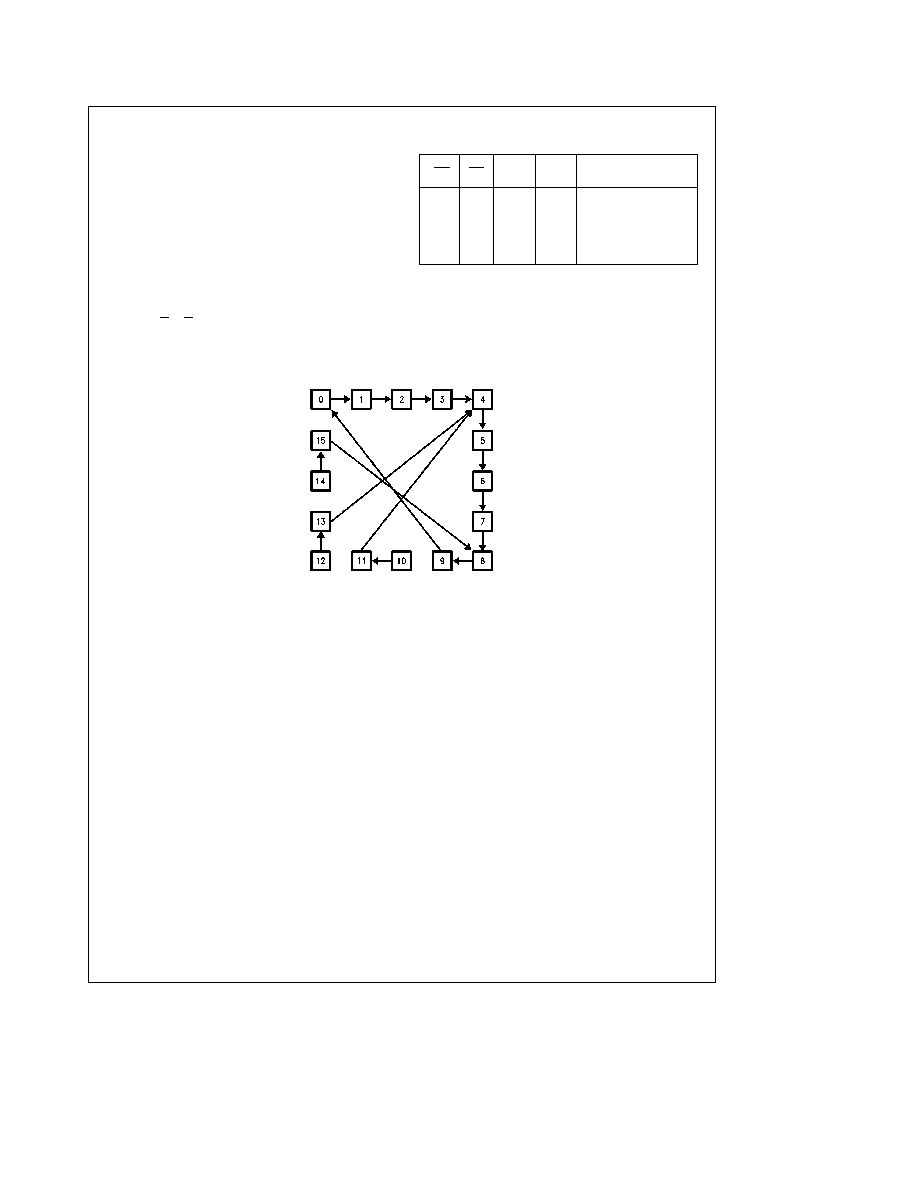
The 'LS160 and 'LS162 count modulo-10 in the BCD (8421)
sequence From state 9 (HLLH) they increment to state 0
(LLLL) The '161 and '163 count modulo-16 binary se-
quence From state 15 (HHHH) they increment to state 0
(LLLL) The clock inputs of all flip-flops are driven in parallel
through a clock buffer Thus all changes of the Q outputs
(except due to Master Reset of the 'LS160) occur as a re-
sult of and synchronous with the LOW-to-HIGH transition
of the CP input signal The circuits have four fundamental
modes of operation in order of precedence asynchronous
reset ('LS160) synchronous reset ('LS162) parallel load
count-up and hold Five control inputs
Master Reset (MR
'LS160) Synchronous Reset (SR 'LS162) Parallel Enable
(PE) Count Enable Parallel (CEP) and Count Enable Trickle
(CET)
determine the mode of operation as shown in the
Mode Select Table A LOW signal on MR overrides all other
inputs and asynchronously forces all outputs LOW A LOW
signal on SR overrides counting and parallel loading and
allows all outputs to go LOW on the next rising edge of CP
A LOW signal on PE overrides counting and allows informa-
tion on the Parallel Data (P
n
) inputs to be loaded into the
flip-flops on the next rising edge of CP With PE and MR
('LS160) or SR ('LS162) HIGH CEP and CET permit count-
ing when both are HIGH Conversely a LOW signal on ei-
ther CEP or CET inhibits counting
The 'LS160A and 'LS162A use D-type edge-triggered flip-
flops and changing the SR PE CEP and CET inputs when
the CP is in either state does not cause errors provided that
the recommended setup and hold times with respect to the
rising edge of CP are observed
3
Functional Description
(Continued)
The Terminal Count (TC) output is HIGH when CET is HIGH
and the counter is in its maximum count state (9 for the
decade counters 15 for the binary counters) To implement
synchronous multistage counters the TC outputs can be
used with the CEP and CET inputs in two different ways
These two schemes are shown in the 9310 data sheet The
TC output is subject to decoding spikes due to internal race
conditions and is therefore not recommended for use as a
clock or asynchronous reset for flip-flops counters or regis-
ters In the decade counters of the 'LS160 'LS162 the TC
output is fully decoded and can only be HIGH in state 9
LOGIC EQUATIONS
Count Enable
e
CEP
CET
PE
TC
e
Q0
Q1
Q2
Q3
CET
Mode Select Table
SR
PE
CET
CEP
Action on the Rising
Clock Edge (
L )
L
X
X
X
RESET (Clear)
H
L
X
X
LOAD (P
n
x
Q
n
)
H
H
H
H
COUNT (Increment)
H
H
L
X
NO CHANGE (Hold)
H
H
X
L
NO CHANGE (Hold)
For the 'LS162
H
e
HIGH Voltage Level
L
e
LOW Voltage Level
X
e
Immaterial
State Diagrams
'LS160 'LS162
TL F 10177 ≠ 5
4

Logic Diagrams
'LS160
TL F 10177 ≠ 3
'LS162
TL F 10177 ≠ 4
5