TL F 6411
DM54LS240DM74LS240
DM54LS241DM74LS241
Octal
TRI-STATE
BuffersLine
DriversLine
Receivers
April 1992
DM54LS240 DM74LS240
DM54LS241 DM74LS241
Octal TRI-STATE
Buffers Line Drivers Line Receivers
General Description
These buffers line drivers are designed to improve both the
performance and PC board density of TRI-STATE buffers
drivers employed as memory-address drivers clock drivers
and bus-oriented transmitters receivers Featuring 400 mV
of hysteresis at each low current PNP data line input they
provide improved noise rejection and high fanout outputs
and can be used to drive terminated lines down to 133X
Features
Y
TRI-STATE outputs drive bus lines directly
Y
PNP inputs reduce DC loading on bus lines
Y
Hysteresis at data inputs improves noise margins
Y
Typical I
OL
(sink current)
54LS
12 mA
74LS
24 mA
Y
Typical I
OH
(source current)
54LS
b
12 mA
74LS
b
15 mA
Y
Typical propagation delay times
Inverting
10 5 ns
Noninverting
12 ns
Y
Typical enable disable time 18 ns
Y
Typical power dissipation (enabled)
Inverting
130 mW
Noninverting
135 mW
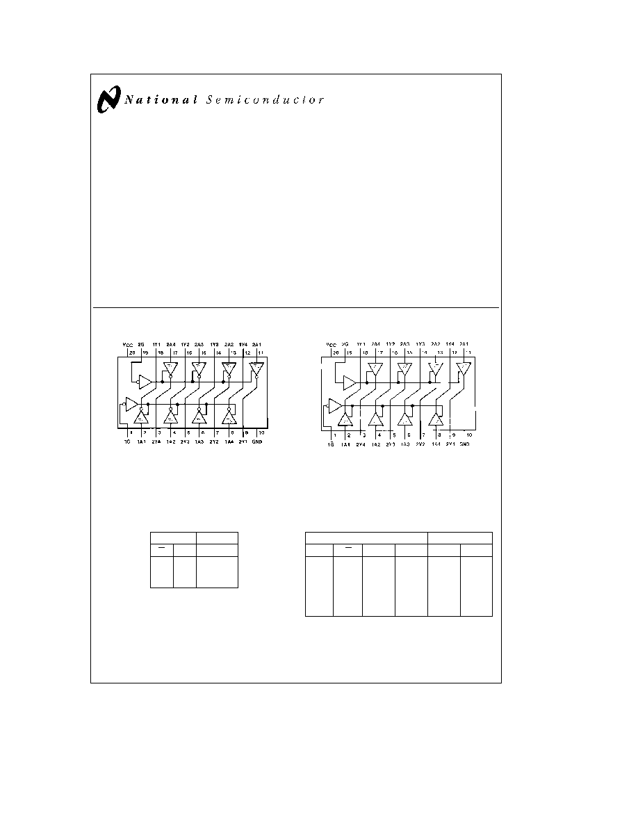
Connection Diagrams
Dual-In-Line Package
TL F 6411 � 1
Dual-In-Line Package
TL F 6411 � 2
Order Number DM54LS240J
DM54LS240W DM54LS240E
DM74LS240WM or DM74LS240N
See NS Package Number E20A J20A
M20B N20A or W20A
Order Number DM54LS241J
DM54LS241W DM54LS241E
DM74LS241WM or DM74LS241N
See NS Package Number E20A J20A
M20B N20A or W20A
Function Tables
LS240
Inputs
Output
G
A
Y
L
L
H
L
H
L
H
X
Z
LS241
Inputs
Outputs
G
G
1A
2A
1Y
2Y
X
L
L
X
L
X
L
H
X
H
X
H
X
X
Z
H
X
X
L
L
H
X
X
H
H
L
X
X
X
Z
L
e
Low Logic Level
H
e
High Logic Level
X
e
Either Low or High Logic Level
Z
e
High Impedance
TRI-STATE
is a registered trademark of National Semiconductor Corporation
C1995 National Semiconductor Corporation
RRD-B30M105 Printed in U S A
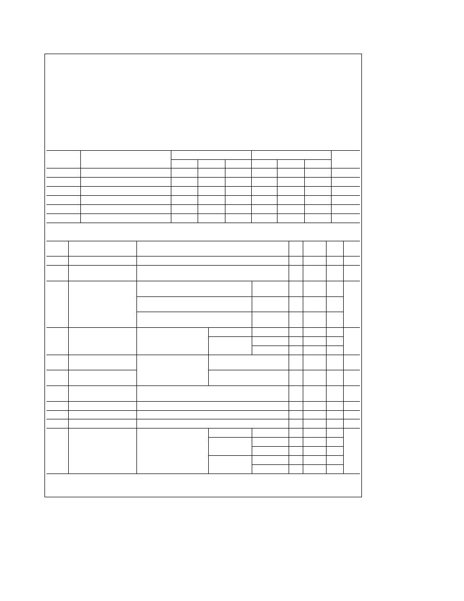
Absolute Maximum Ratings
(Note)
If Military Aerospace specified devices are required
please contact the National Semiconductor Sales
Office Distributors for availability and specifications
Supply Voltage
7V
Input Voltage
7V
Operating Free Air Temperature Range
DM54LS 54LS
b
55 C to
a
125 C
DM74LS
0 C to
a
70 C
Storage Temperature Range
b
65 C to
a
150 C
Note
The ``Absolute Maximum Ratings'' are those values
beyond which the safety of the device cannot be guaran-
teed The device should not be operated at these limits The
parametric values defined in the ``Electrical Characteristics''
table are not guaranteed at the absolute maximum ratings
The ``Recommended Operating Conditions'' table will define
the conditions for actual device operation
Recommended Operating Conditions
Symbol
Parameter
DM54LS240 241
DM74LS240 241
Units
Min
Nom
Max
Min
Nom
Max
V
CC
Supply Voltage
4 5
5
5 5
4 75
5
5 25
V
V
IH
High Level Input Voltage
2
2
V
V
IL
Low Level Input Voltage
0 7
0 8
V
I
OH
High Level Output Current
b
12
b
15
mA
I
OL
Low Level Output Current
12
24
mA
T
A
Free Air Operating Temperature
b
55
125
0
70
C
Electrical Characteristics
over recommended operating free air temperature range (unless otherwise noted)
Symbol
Parameter
Conditions
Min
Typ
Max
Units
(Note 1)
V
I
Input Clamp Voltage
V
CC
e
Min I
I
e b
18 mA
b
1 5
V
HYS
Hysteresis (V
Ta
b
V
Tb
)
V
CC
e
Min
0 2
0 4
V
Data Inputs Only
V
OH
High Level Output Voltage
V
CC
e
Min V
IH
e
Min
DM74
2 7
V
IL
e
Max I
OH
e b
1 mA
V
CC
e
Min V
IH
e
Min
DM54 DM74
2 4
3 4
V
V
IL
e
Max I
OH
e b
3 mA
V
CC
e
Min V
IH
e
Min
DM54 DM74
2
V
IL
e
0 5V I
OH
e
Max
V
OL
Low Level Output Voltage
V
CC
e
Min
I
OL
e
12 mA
DM74
0 4
V
IL
e
Max
I
OL
e
Max
DM54
0 4
V
V
IH
e
Min
DM74
0 5
I
OZH
Off-State Output Current
V
CC
e
Max
V
O
e
2 7V
20
m
A
High Level Voltage Applied V
IL
e
Max
I
OZL
Off-State Output Current
V
IH
e
Min
V
O
e
0 4V
b
20
m
A
Low Level Voltage Applied
I
I
Input Current at Maximum
V
CC
e
Max V
I
e
7V (DM74)
0 1
mA
Input Voltage
V
I
e
10V (DM54)
I
IH
High Level Input Current
V
CC
e
Max V
I
e
2 7V
20
m
A
I
IL
Low Level Input Current
V
CC
e
Max V
I
e
0 4V
b
0 2
mA
I
OS
Short Circuit Output Current V
CC
e
Max (Note 2)
b
40
b
225
mA
I
CC
Supply Current
V
CC
e
Max
Outputs High
LS240 LS241
13
23
Outputs Open
Outputs Low
LS240
26
44
LS241
27
46
mA
Outputs Disabled LS240
29
50
LS241
32
54
Note 1
All typicals are at V
CC
e
5V T
A
e
25 C
Note 2
Not more than one output should be shorted at a time and the duration should not exceed one second
2
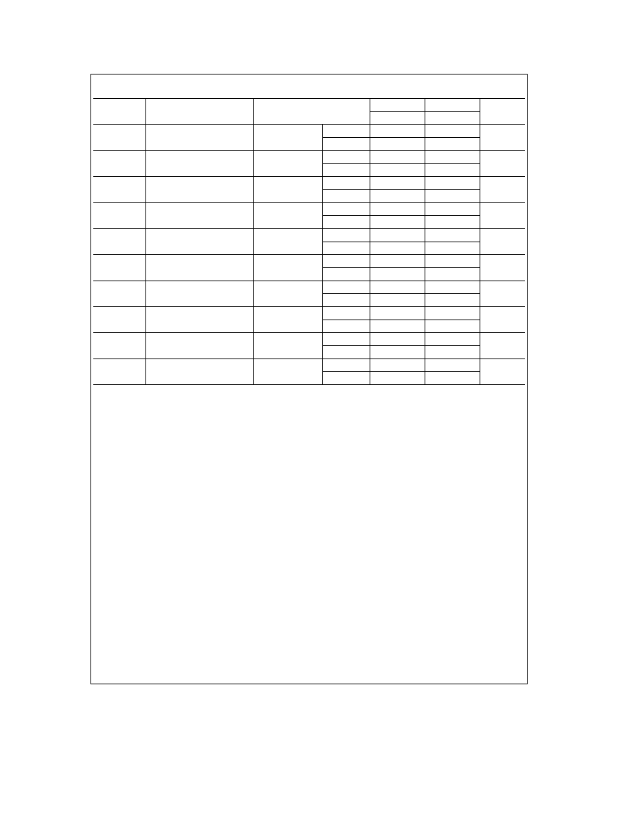
Switching Characteristics
at V
CC
e
5V and T
A
e
25 C
Symbol
Parameter
Conditions
DM54LS
DM74LS
Units
Max
Max
t
PLH
Propagation Delay Time
C
L
e
45 pF
LS240
18
14
ns
Low to High Level Output
R
L
e
667X
LS241
18
18
t
PHL
Propagation Delay Time
C
L
e
45 pF
LS240
18
18
ns
High to Low Level Output
R
L
e
667X
LS241
18
18
t
PZL
Output Enable Time to
C
L
e
45 pF
LS240
30
30
ns
Low Level
R
L
e
667X
LS241
30
30
t
PZH
Output Enable Time to
C
L
e
45 pF
LS240
23
23
ns
High Level
R
L
e
667X
LS241
23
23
t
PLZ
Output Disable Time
C
L
e
5 pF
LS240
25
25
ns
from Low Level
R
L
e
667X
LS241
25
25
t
PHZ
Output Disable Time
C
L
e
5 pF
LS240
18
18
ns
from High Level
R
L
e
667X
LS241
18
18
t
PLH
Propagation Delay Time
C
L
e
150 pF
LS240
18
ns
Low to High Level Output
R
L
e
667X
LS241
21
t
PHL
Propagation Delay Time
C
L
e
150 pF
LS240
22
ns
High to Low Level Output
R
L
e
667X
LS241
22
t
PZL
Output Enable Time to
C
L
e
150 pF
LS240
33
ns
Low Level
R
L
e
667X
LS241
33
t
PZH
Output Enable Time to
C
L
e
150 pF
LS240
26
ns
High Level
R
L
e
667X
LS241
26
Note
54LS Output load is C
L
e
50 pF for t
PLH
t
PHL
t
PZL
and t
PZH
3
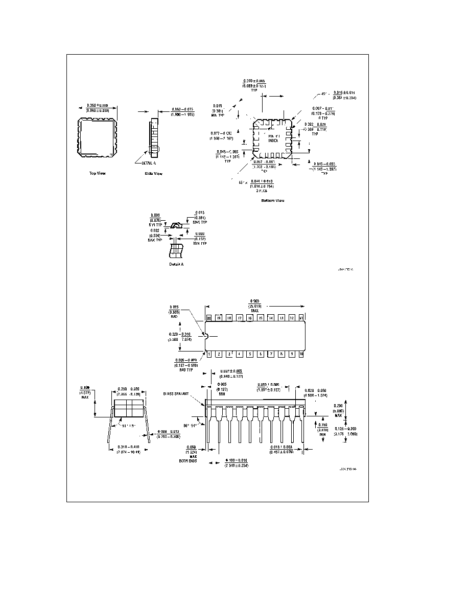
Physical Dimensions
inches (millimeters)
Ceramic Leadless Chip Carrier Package (E)
Order Number DM54LS240E or DM54LS241E
NS Package Number E20A
20-Lead Ceramic Dual-In-Line Package (J)
Order Number DM54LS240J or DM54LS241J
NS Package Number J20A
4
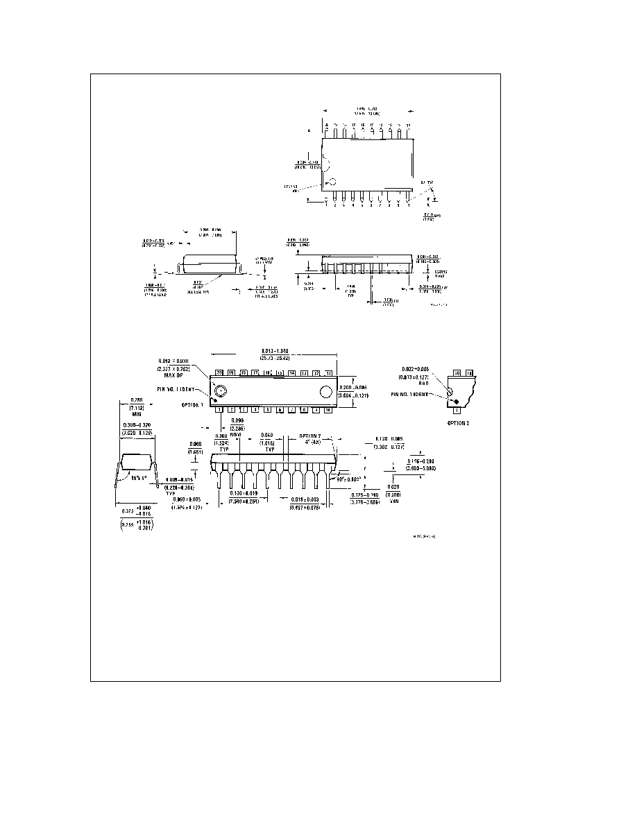
Physical Dimensions
inches (millimeters) (Continued)
20-Lead Wide Small Outline Molded Package (M)
Order Number DM74LS240WM or DM74LS241WM
NS Package Number M20B
20-Lead Molded Dual-In-Line Package (N)
Order Number DM74LS240N or DM74LS241N
NS Package Number N20A
5