TL F 8442
54LS244DM74LS244
Octal
TRI-STATE
BuffersLine
DriversLine
Receivers
August 1989
54LS244 DM74LS244 Octal TRI-STATE
Buffers Line Drivers Line Receivers
General Description
These buffers line drivers are designed to improve both the
performance and PC board density of TRI-STATE buffers
drivers employed as memory-address drivers clock drivers
and bus-oriented transmitters receivers Featuring 400 mV
of hysteresis at each low current PNP data line input they
provide improved noise rejection and high fanout outputs
and can be used to drive terminated lines down to 133X
Features
Y
TRI-STATE outputs drive bus lines directly
Y
PNP inputs reduce DC loading on bus lines
Y
Hysteresis at data inputs improves noise margins
Y
Typical I
OL
(sink current)
54LS
12 mA
74LS
24 mA
Y
Typical I
OH
(source current)
54LS
b
12 mA
74LS
b
15 mA
Y
Typical propagation delay times
Inverting
10 5 ns
Noninverting
12 ns
Y
Typical enable disable time 18 ns
Y
Typical power dissipation (enabled)
Inverting
130 mW
Noninverting
135 mW
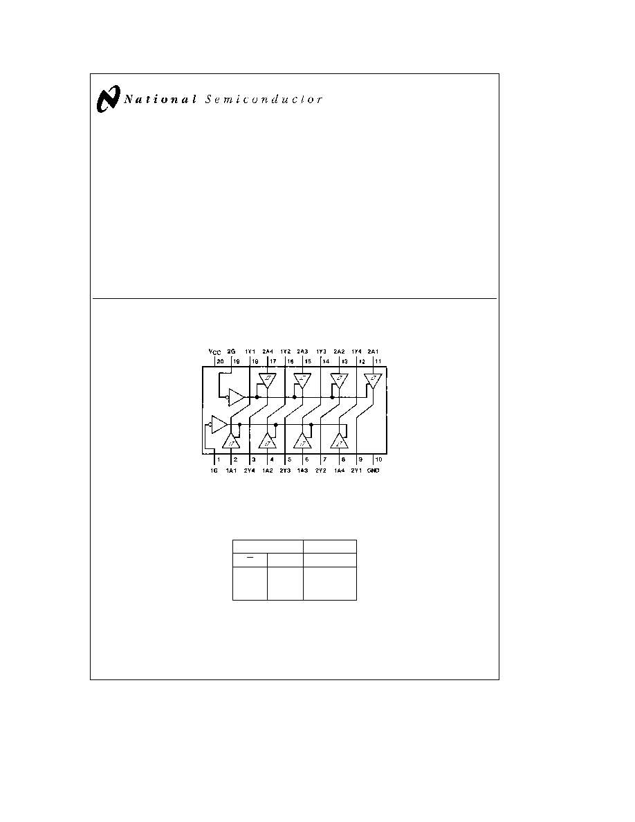
Connection Diagram
Dual-In-Line Package
TL F 8442 � 1
Order Number 54LS244DMQB 54LS244FMQB 54LS244LMQB
DM74LS244WM or DM74LS244N
See NS Package Number E20A J20A M20B N20A or W20A
Function Table
Inputs
Output
G
A
Y
L
L
L
L
H
H
H
X
Z
L
e
Low Logic Level
H
e
High Logic Level
X
e
Either Low or High Logic Level
Z
e
High Impedance
TRI-STATE
is a registered trademark of National Semiconductor Corporation
C1995 National Semiconductor Corporation
RRD-B30M105 Printed in U S A

Absolute Maximum Ratings
(Note)
If Military Aerospace specified devices are required
please contact the National Semiconductor Sales
Office Distributors for availability and specifications
Supply Voltage
7V
Input Voltage
7V
Operating Free Air Temperature Range
54LS
b
55 C to
a
125 C
DM74LS
0 C to
a
70 C
Storage Temperature Range
b
65 C to
a
150 C
Note
The ``Absolute Maximum Ratings'' are those values
beyond which the safety of the device cannot be guaran-
teed The device should not be operated at these limits The
parametric values defined in the ``Electrical Characteristics''
table are not guaranteed at the absolute maximum ratings
The ``Recommended Operating Conditions'' table will define
the conditions for actual device operation
Recommended Operating Conditions
Symbol
Parameter
54LS244
DM74LS244
Units
Min
Nom
Max
Min
Nom
Max
V
CC
Supply Voltage
4 5
5
5 5
4 75
5
5 25
V
V
IH
High Level Input Voltage
2
2
V
V
IL
Low Level Input Voltage
0 7
0 8
V
I
OH
High Level Output Current
b
12
b
15
mA
I
OL
Low Level Output Current
12
24
mA
T
A
Free Air Operating Temperature
b
55
125
0
70
C
Electrical Characteristics
over recommended operating free air temperature range (unless otherwise noted)
Symbol
Parameter
Conditions
Min
Typ
Max
Units
(Note 1)
V
I
Input Clamp Voltage
V
CC
e
Min I
I
e b
18 mA
b
1 5
V
HYS
Hysteresis (V
Ta
b
V
Tb
)
V
CC
e
Min
0 2
0 4
V
Data Inputs Only
V
OH
High Level Output Voltage
V
CC
e
Min V
IH
e
Min
DM74
2 7
V
IL
e
Max I
OH
e b
1 mA
V
CC
e
Min V
IH
e
Min
54LS DM74
2 4
3 4
V
V
IL
e
Max I
OH
e b
3 mA
V
CC
e
Min V
IH
e
Min
54LS DM74
2
V
IL
e
0 5V I
OH
e
Max
V
OL
Low Level Output Voltage
V
CC
e
Min
I
OL
e
12 mA
54LS DM74
0 4
V
IL
e
Max
V
I
OL
e
Max
DM74
0 5
V
IH
e
Min
I
OZH
Off-State Output Current
V
CC
e
Max
V
O
e
2 7V
20
m
A
High Level Voltage Applied
V
IL
e
Max
I
OZL
Off-State Output Current
V
IH
e
Min
V
O
e
0 4V
b
20
m
A
Low Level Voltage Applied
I
I
Input Current at Maximum
V
CC
e
Max
V
I
e
7V (DM74)
0 1
mA
Input Voltage
V
I
e
10V (54LS)
I
IH
High Level Input Current
V
CC
e
Max
V
I
e
2 7V
20
m
A
I
IL
Low Level Input Current
V
CC
e
Max
V
I
e
0 4V
b
0 5
b
200
m
A
I
OS
Short Circuit Output Current
V
CC
e
Max (Note 2)
54LS
b
50
b
225
mA
DM74
b
40
I
CC
Supply Current
V
CC
e
Max
Outputs High
13
23
Outputs Open
Outputs Low
27
46
mA
Outputs Disabled
32
54
Note 1
All typicals are at V
CC
e
5V T
A
e
25 C
Note 2
Not more than one output should be shorted at a time and the duration should not exceed one second
2

Switching Characteristics
at V
CC
e
5V T
A
e
25 C (see Section 1 for Test Waveforms and Output Load)
Symbol
Parameter
Conditions
54LS Max
DM74LS Max
Units
t
PLH
Propagation Delay Time
C
L
e
45 pF
18
18
ns
Low to High Level Output
R
L
e
667X
t
PHL
Propagation Delay Time
C
L
e
45 pF
18
18
ns
High to Low Level Output
R
L
e
667X
t
PZL
Output Enable Time to
C
L
e
45 pF
30
30
ns
Low Level
R
L
e
667X
t
PZH
Output Enable Time to
C
L
e
45 pF
23
23
ns
High Level
R
L
e
667X
t
PLZ
Output Disable Time
C
L
e
5 pF
25
25
ns
from Low Level
R
L
e
667X
t
PHZ
Output Disable Time
C
L
e
5 pF
18
18
ns
from High Level
R
L
e
667X
t
PLH
Propagation Delay Time
C
L
e
150 pF
21
ns
Low to High Level Output
R
L
e
667X
t
PHL
Propagation Delay Time
C
L
e
150 pF
22
ns
High to Low Level Output
R
L
e
667X
t
PZL
Output Enable Time to
C
L
e
150 pF
33
ns
Low Level
R
L
e
667X
t
PZH
Output Enable Time to
C
L
e
150 pF
26
ns
High Level
R
L
e
667X
Note
54LS Output Load is C
L
e
50 pF for t
PLH
t
PHL
t
PZL
and t
PZH
3
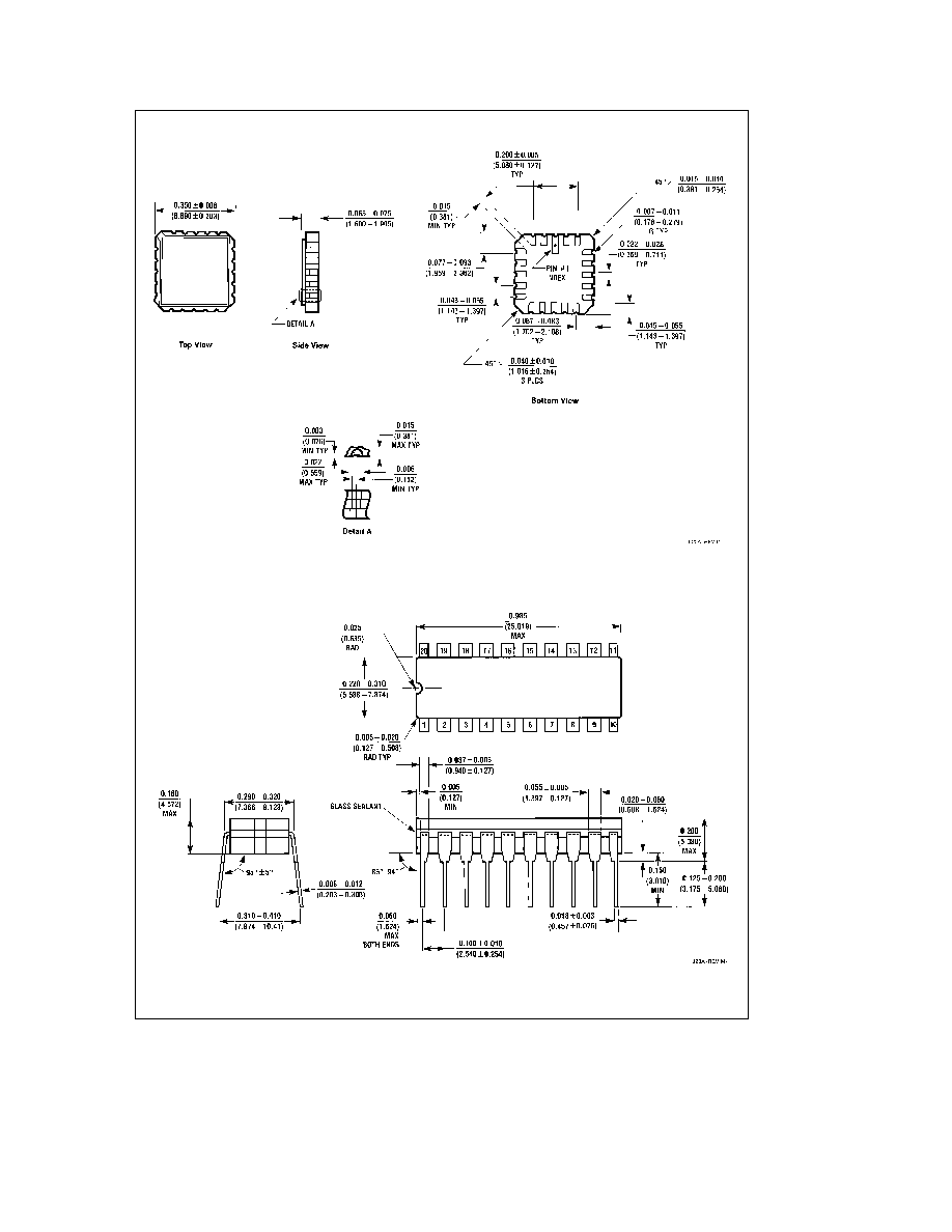
Physical Dimensions
inches (millimeters)
Ceramic Leadless Chip Carrier Package (E)
Order Number 54LS244LMQB
NS Package Number E20A
20-Lead Ceramic Dual-In-Line Package (J)
Order Number 54LS244DMQB
NS Package Number J20A
4
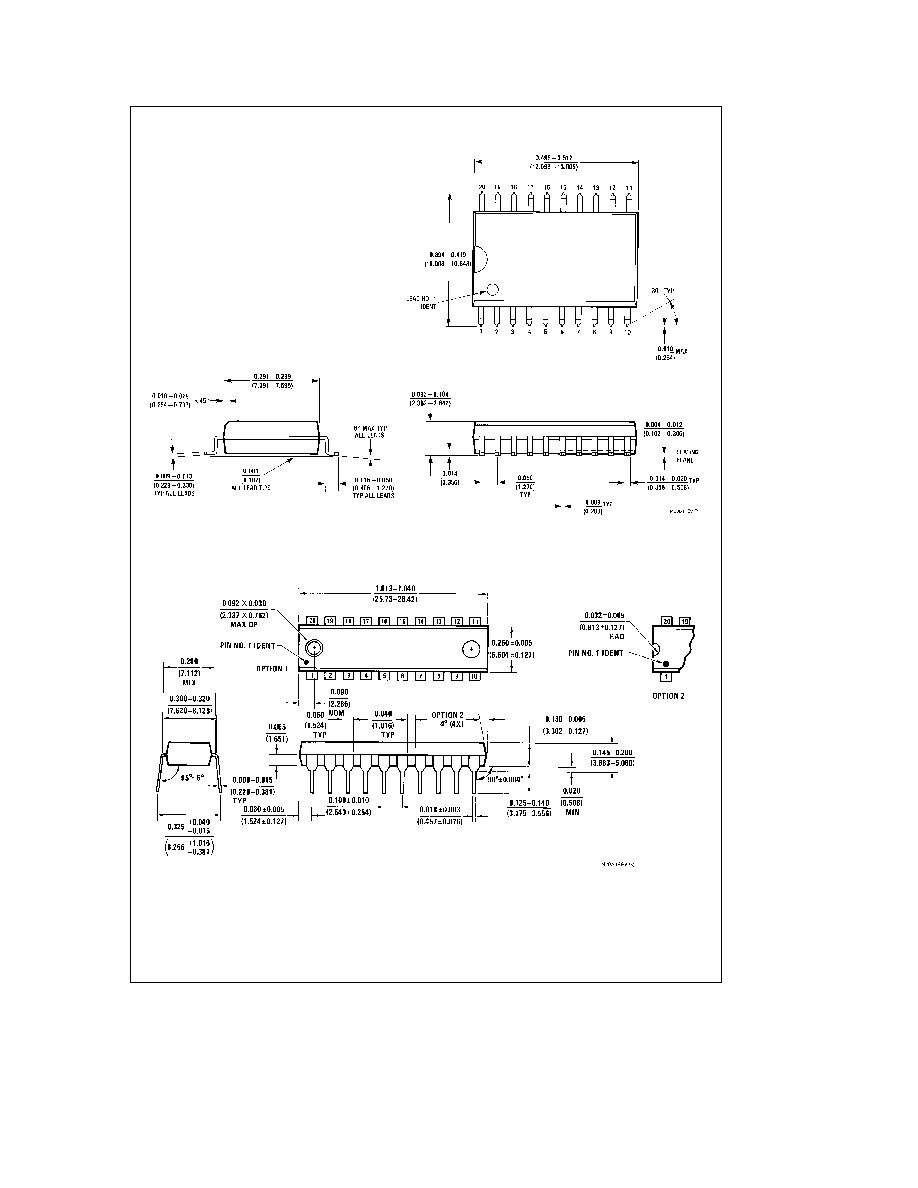
Physical Dimensions
inches (millimeters) (Continued)
20-Lead Wide Small Outline Molded Package (M)
Order Number DM74LS244WM
NS Package Number M20B
20-Lead Molded Dual-In-Line Package (N)
Order Number DM74LS244N
NS Package Number N20A
5

54LS244DM74LS244
Octal
TRI-STATE
BuffersLine
DriversLine
Receivers
Physical Dimensions
inches (millimeters) (Continued)
20-Lead Ceramic Flat Package (W)
Order Number 54LS244FMQB
NS Package Number W20A
LIFE SUPPORT POLICY
NATIONAL'S PRODUCTS ARE NOT AUTHORIZED FOR USE AS CRITICAL COMPONENTS IN LIFE SUPPORT
DEVICES OR SYSTEMS WITHOUT THE EXPRESS WRITTEN APPROVAL OF THE PRESIDENT OF NATIONAL
SEMICONDUCTOR CORPORATION As used herein
1 Life support devices or systems are devices or
2 A critical component is any component of a life
systems which (a) are intended for surgical implant
support device or system whose failure to perform can
into the body or (b) support or sustain life and whose
be reasonably expected to cause the failure of the life
failure to perform when properly used in accordance
support device or system or to affect its safety or
with instructions for use provided in the labeling can
effectiveness
be reasonably expected to result in a significant injury
to the user
National Semiconductor
National Semiconductor
National Semiconductor
National Semiconductor
Corporation
Europe
Hong Kong Ltd
Japan Ltd
1111 West Bardin Road
Fax (a49) 0-180-530 85 86
13th Floor Straight Block
Tel 81-043-299-2309
Arlington TX 76017
Email cnjwge tevm2 nsc com
Ocean Centre 5 Canton Rd
Fax 81-043-299-2408
Tel 1(800) 272-9959
Deutsch Tel (a49) 0-180-530 85 85
Tsimshatsui Kowloon
Fax 1(800) 737-7018
English
Tel (a49) 0-180-532 78 32
Hong Kong
Fran ais Tel (a49) 0-180-532 93 58
Tel (852) 2737-1600
Italiano
Tel (a49) 0-180-534 16 80
Fax (852) 2736-9960
National does not assume any responsibility for use of any circuitry described no circuit patent licenses are implied and National reserves the right at any time without notice to change said circuitry and specifications