TL F 10213
DM74LS249
BCD
to
7-Segment
Decoder
with
Open-Collector
Outputs
February 1992
DM74LS249
BCD to 7-Segment Decoder with Open-Collector Outputs
General Description
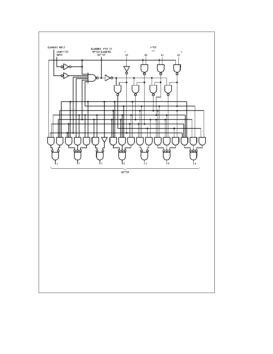
The 'LS249 has active HIGH open-collector outputs and in-
corporates the Lamp Test and BI RBO inputs Additionally
the 'LS249 will light the top bar (segment a) for numeral 6
and the bottom bar (segment d) for numeral 9
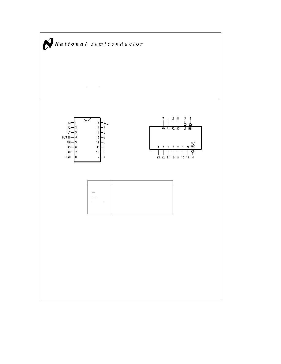
Connection Diagram
Dual-In-Line Package
TL F 10213 ≠ 1
Order Number DM74LS249N
See NS Package Number N16E
Logic Symbol
TL F 10213 ≠ 2
V
CC
e
Pin 16
GND
e
Pin 8
Pin Names
Description
A
0
≠ A
3
BCD Inputs
BI
Blanking Input (Active LOW)
LT
Lamp Test Input (Active LOW)
BI RBO
Blanking Input (Active LOW) or
Ripple Blanking Output (Active LOW)
a ≠ g
Segment Outputs (Active HIGH)
C1995 National Semiconductor Corporation
RRD-B30M105 Printed in U S A
Absolute Maximum Ratings
(Note)
Supply Voltage
7V
Input Voltage
7V
Operating Free Air Temperature Range
0 C to
a
70 C
Storage Temperature Range
b
65 C to
a
150 C
Note
The ``Absolute Maximum Ratings'' are those values
beyond which the safety of the device cannot be guaran-
teed The device should not be operated at these limits The
parametric values defined in the ``Electrical Characteristics''
table are not guaranteed at the absolute maximum ratings
The ``Recommended Operating Conditions'' table will define
the conditions for actual device operation
Recommended Operating Conditions
Symbol
Parameter
Min
Nom
Max
Units
V
CC
Supply Voltage
4 75
5
5 25
V
V
IH
High Level Input Voltage
2
V
V
IL
Low Level Input Voltage
0 8
V
I
OH
High Level Output Current (BI RBO)
b
0 25
mA
I
OL
Low Level Output Current
8
mA
T
A
Free Air Operating Temperature
0
70
C
Electrical Characteristics
over recommended operating free air temperature range (unless otherwise noted)
Symbol
Parameter
Conditions
Min
Typ
Max
Units
(Note 1)
V
I
Input Clamp Voltage
V
CC
e
Min I
I
e b
18 mA
b
1 5
V
V
OH
High Level Output Voltage
V
CC
e
Min I
OH
e
Max
2 7
3 4
V
(BI RBO)
V
IL
e
Max
I
CEX
High Level Output Current
V
CC
e
Min V
O
e
5 5V
250
m
A
(a thru g)
V
OL
Low Level Output Voltage
V
CC
e
Min I
OL
e
Max
0 35
0 5
V
IH
e
Min
V
I
OL
e
4 mA V
CC
e
Min
0 25
0 4
I
I
Input Current
Max
V
CC
e
Max V
I
e
7V
0 1
mA
Input Voltage
I
IH
High Level Input Current
V
CC
e
Max V
I
e
2 7V
20
m
A
I
IL
Low Level Input Current
V
CC
e
Max V
I
e
0 4V
Inputs
b
0 4
mA
BI RBO
b
1 2
I
OS
Short Circuit Output Current
V
CC
e
Max (Note 2)
b
0 3
b
2 0
mA
I
CC
Supply Current
V
CC
e
Max V
IN
e
4 5V
15
mA
Note 1
All typicals are at V
CC
e
5V T
A
e
25 C
Note 2
Not more than one output should be shorted at a time and the duration should not exceed one second
2
Switching Characteristics
V
CC
e a
5 0V T
A
e a
25 C
R
L
e
2 kX
Symbol
Parameter
C
L
e
15 pF
Units
Min
Max
t
PLH
Propagation Delay Time
100
ns
t
PHL
A
n
to a ≠ g (54LS R
L
e
2 kX)
100
t
PLH
Propagation Delay Time
100
ns
t
PHL
BI to a ≠ g (54LS R
L
e
6 kX)
100
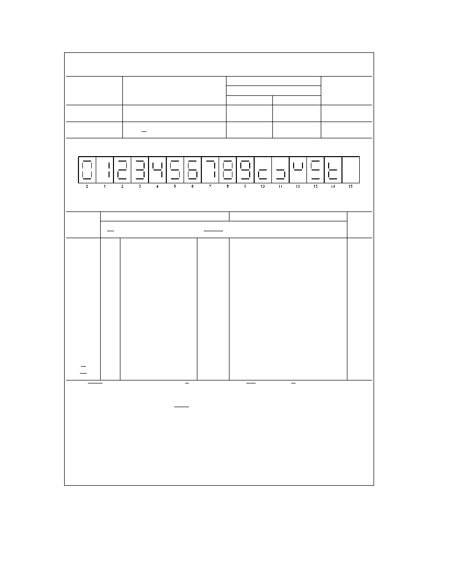
Numerical Designations
Resultant Displays
TL F 10213 ≠ 3
Truth Table
Decimal
Inputs
Outputs
or
Note
Function
LT
A
3
A
2
A
1
A
0
BI RBO
a
b
c
d
e
f
g
0
H
L
L
L
L
H
H
H
H
H
H
H
L
1
1
H
L
L
L
H
H
L
H
H
L
L
L
L
1
2
H
L
L
H
L
H
H
H
L
H
H
L
H
3
H
L
L
H
H
H
H
H
H
H
L
L
H
4
H
L
H
L
L
H
L
H
H
L
L
H
H
5
H
L
H
L
H
H
H
L
H
H
L
H
H
6
H
L
H
H
L
H
L
L
H
H
H
H
H
7
H
L
H
H
H
H
H
H
H
L
L
L
L
8
H
H
L
L
L
H
H
H
H
H
H
H
H
9
H
H
L
L
H
H
H
H
H
L
L
H
H
10
H
H
L
H
L
H
L
L
L
H
H
L
H
11
H
H
L
H
H
H
L
L
H
H
L
L
H
12
H
H
H
L
L
H
L
H
L
L
L
H
H
13
H
H
H
L
H
H
H
L
L
H
L
H
H
14
H
H
H
H
L
H
L
L
L
H
H
H
H
15
H
H
H
H
H
H
L
L
L
L
L
L
L
BI
X
X
X
X
X
L
L
L
L
L
L
L
L
2
LT
L
X
X
X
X
H
H
H
H
H
H
H
H
3
Note 1
BI RBO is wired-AND logic serving as blanking input (BI) and or ripple-blanking output (RBO) The blanking out (BI) must be open or held at a HIGH level
when output functions 0 through 15 are desired X
e
input may be HIGH or LOW
Note 2
When a LOW level is applied to the blanking input (forced condition) all segment outputs go to a LOW level regardless of the state of any other input
condition
Note 3
When the blanking input ripple-blanking output (BI RBO) is open or held at a HIGH level and a LOW level is applied to lamp test input all segment outputs
go to a HIGH level
3