TL F 6417
54LS257ADM54LS257BDM74LS257B
54LS258ADM54LS258BDM74LS258B
TRI-STATE
Quad
2-Data
SelectorsMultiplexers
June 1989
54LS257A DM54LS257B DM74LS257B
54LS258A DM54LS258B DM74LS258B
TRI-STATE
Quad 2-Data Selectors Multiplexers
General Description
These Schottky-clamped high-performance multiplexers
feature TRI-STATE outputs that can interface directly with
data lines of bus-organized systems With all but one of the
common outputs disabled (at a high impedance state) the
low impedance of the single enabled output will drive the
bus line to a high or low logic level To minimize the possibil-
ity that two outputs will attempt to take a common bus to
opposite logic levels the output enable circuitry is designed
such that the output disable times are shorter than the out-
put enable times
This TRI-STATE output feature means that n-bit (paralleled)
data selectors with up to 258 sources can be implemented
for data buses It also permits the use of standard TTL reg-
isters for data retention throughout the system
Features
Y
TRI-STATE versions LS157 and LS158 with same pin-
outs
Y
Schottky-clamped for significant improvement in A-C
performance
Y
Provides bus interface from multiple sources in high-
performance systems
Y
Average propagation delay from data input 12 ns
Y
Typical power dissipation
LS257B
50 mW
LS258B
35 mW
Y
Alternate
military aerospace
devices
(54LS257A
54LS258A) are available Contact a National Semicon-
ductor Sales Office Distributor for specifications
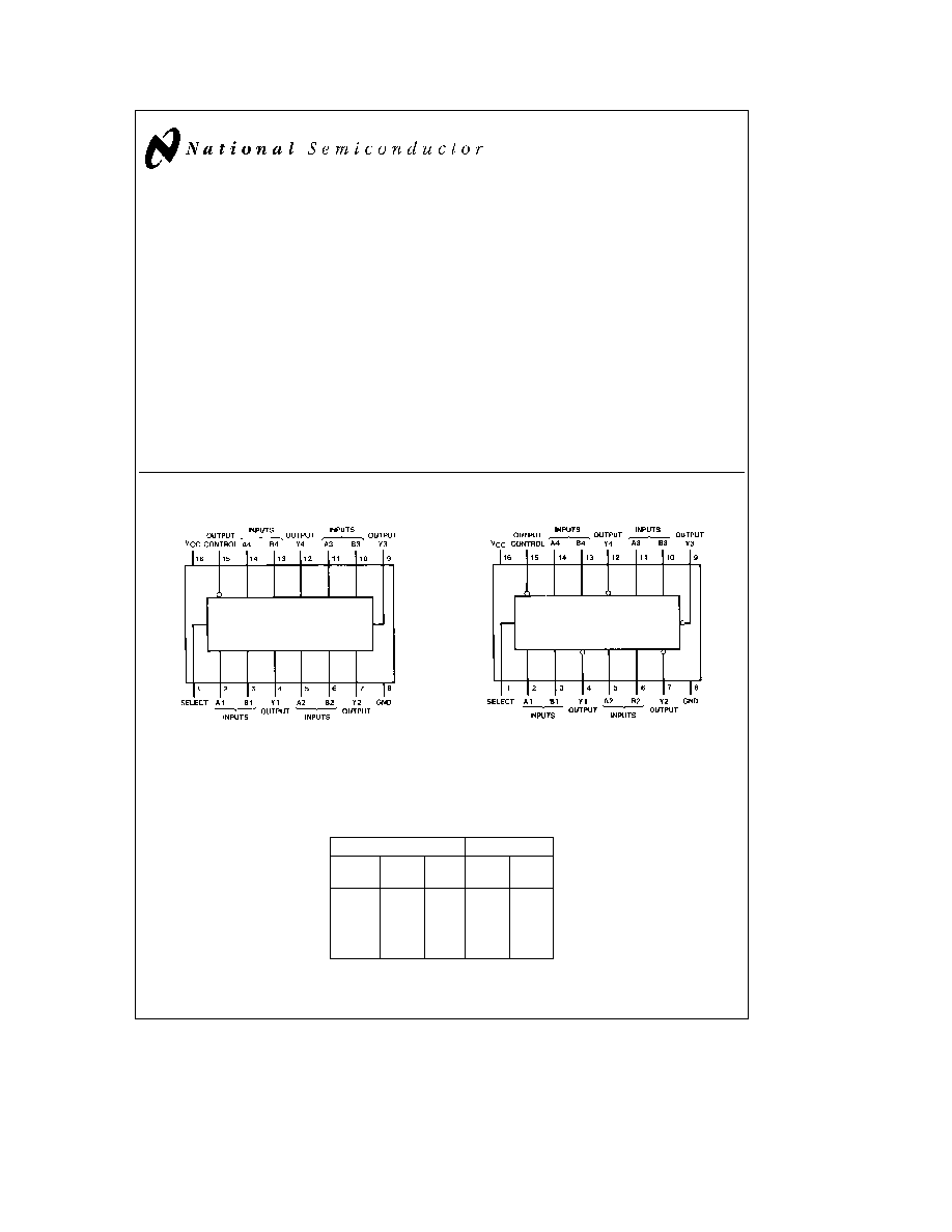
Connection Diagrams
Dual-In-Line Package
TL F 6417 ≠ 1
Order Number 54LS257ADMQB 54LS257AFMQB
54LS257ALMQB DM54LS257BJ DM54LS257BW
DM74LS257BM or DM74LS257BN
See NS Package Number E20A J16A
M16A N16E or W16A
Dual-In-Line Package
TL F 6417 ≠ 2
Order Number 54LS258ADMQB 54LS258AFMQB
54LS258ALMQB DM54LS258BJ DM54LS258BW
DM74LS258BM or DM74LS258BN
See NS Package Number E20A J16A
M16A N16E or W16A
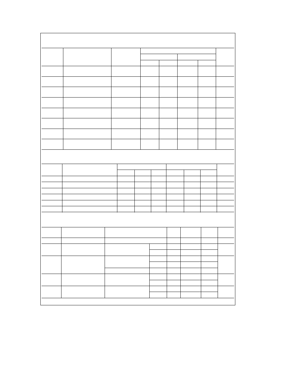
Function Table
Inputs
Output Y
Output
Select
A
B
LS257
LS258
Control
H
X
X
X
Z
Z
L
L
L
X
L
H
L
L
H
X
H
L
L
H
X
L
L
H
L
H
X
H
H
L
H
e
High Level L
e
Low Level X
e
Don't Care
Z
e
High Impedance (off)
TRI-STATE
is a registered trademark of National Semiconductor Corporation
C1995 National Semiconductor Corporation
RRD-B30M105 Printed in U S A

Absolute Maximum Ratings
(Note)
If Military Aerospace specified devices are required
please contact the National Semiconductor Sales
Office Distributors for availability and specifications
Supply Voltage
7V
Input Voltage
7V
Operating Free Air Temperature Range
DM54LS and 54LS
b
55 C to
a
125 C
DM74LS
0 C to
a
70 C
Storage Temperature Range
b
65 C to
a
150 C
Note
The ``Absolute Maximum Ratings'' are those values
beyond which the safety of the device cannot be guaran-
teed The device should not be operated at these limits The
parametric values defined in the ``Electrical Characteristics''
table are not guaranteed at the absolute maximum ratings
The ``Recommended Operating Conditions'' table will define
the conditions for actual device operation
Recommended Operating Conditions
Symbol
Parameter
DM54LS257B
DM74LS257B
Units
Min
Nom
Max
Min
Nom
Max
V
CC
Supply Voltage
4 5
5
5 5
4 75
5
5 25
V
V
IH
High Level Input Voltage
2
2
V
V
IL
Low Level Input Voltage
0 7
0 8
V
I
OH
High Level Output Current
b
1
b
2 6
mA
I
OL
Low Level Output Current
12
24
mA
T
A
Free Air Operating Temperature
b
55
125
0
70
C
'LS257B Electrical Characteristics
over recommended operating free air temperature range (unless otherwise noted)
Symbol
Parameter
Conditions
Min
Typ
Max
Units
(Note 1)
V
I
Input Clamp Voltage
V
CC
e
Min I
I
e b
18 mA
b
1 5
V
V
OH
High Level Output
V
CC
e
Min I
OH
e
Max
DM54
2 4
3 4
V
Voltage
V
IL
e
Max V
IH
e
Min
DM74
2 4
3 1
V
OL
Low Level Output
V
CC
e
Min I
OL
e
Max
DM54
0 25
0 4
Voltage
V
IL
e
Max V
IH
e
Min
DM74
0 35
0 5
V
I
OL
e
12 mA V
CC
e
Min
DM74
0 25
0 4
I
I
Input Current
Max
V
CC
e
Max
Select
0 2
mA
Input Voltage
V
I
e
7V
Other
0 1
I
IH
High Level Input
V
CC
e
Max
Select
40
m
A
Current
V
I
e
2 7V
Other
20
I
IL
Low Level Input
V
CC
e
Max
Select
b
0 8
mA
Current
V
I
e
0 4V
Other
b
0 4
I
OZH
Off-State Output Current
V
CC
e
Max V
O
e
2 7V
with High Level Output
V
IH
e
Min V
IL
e
Max
20
m
A
Voltage Applied
I
OZL
Off-State Output Current
V
CC
e
Max V
O
e
0 4V
with Low Level Output
V
IH
e
Min V
IL
e
Max
b
20
m
A
Voltage Applied
I
OS
Short Circuit
V
CC
e
Max
DM54
b
20
b
100
mA
Output Current
(Note 2)
DM74
b
20
b
100
I
CCH
Supply Current with
V
CC
e
Max (Note 3)
5 9
10
mA
Outputs High
I
CCL
Supply Current with
V
CC
e
Max (Note 3)
9 2
16
mA
Outputs Low
I
CCZ
Supply Current with
V
CC
e
Max (Note 3)
12
19
mA
Outputs Disabled
Note 1
All typicals are at V
CC
e
5V T
A
e
25 C
Note 2
Not more than one output should be shorted at a time and the duration should not exceed one second
Note 3
I
CC
is measured with all outputs open and all possible inputs grounded while achieving the stated output conditions
2
'LS257B Switching Characteristics
at V
CC
e
5V and T
A
e
25 C (See Section 1 for Test Waveforms and Output Load)
From (Input)
R
L
e
667X
Symbol
Parameter
To (Output)
C
L
e
45 pF
C
L
e
150 pF
Units
Min
Max
Min
Max
t
PLH
Propagation Delay Time
Data to
18
27
ns
Low to High Level Output
Output
t
PHL
Propagation Delay Time
Data to
18
27
ns
High to Low Level Output
Output
t
PLH
Propagation Delay Time
Select to
28
35
ns
Low to High Level Output
Output
t
PHL
Propagation Delay Time
Select to
35
42
ns
High to Low Level Output
Output
t
PZH
Output Enable Time
Output
15
27
ns
to High Level Output
Control to Y
t
PZL
Output Enable Time
Output
28
38
ns
to Low Level Output
Control to Y
t
PHZ
Output Disable Time from
Output
26
ns
High Level Output (Note 1)
Control to Y
t
PLZ
Output Disable Time from
Output
25
ns
Low Level Output (Note 1)
Control to Y
Note 1
C
L
e
5 pF
Recommended Operating Conditions
Symbol
Parameter
DM54LS258B
DM74LS258B
Units
Min
Nom
Max
Min
Nom
Max
V
CC
Supply Voltage
4 5
5
5 5
4 75
5
5 25
V
V
IH
High Level Input Voltage
2
2
V
V
IL
Low Level Input Voltage
0 7
0 8
V
I
OH
High Level Output Current
b
1
b
2 6
mA
I
OL
Low Level Output Current
12
24
mA
T
A
Free Air Operating Temperature
b
55
125
0
70
C
'LS258B Electrical Characteristics
over recommended operating free air temperature range (unless otherwise noted)
Symbol
Parameter
Conditions
Min
Typ
Max
Units
(Note 1)
V
I
Input Clamp Voltage
V
CC
e
Min I
I
e b
18 mA
b
1 5
V
V
OH
High Level Output
V
CC
e
Min I
OH
e
Max
DM54
2 4
3 4
V
Voltage
V
IL
e
Max V
IH
e
Min
DM74
2 4
3 1
V
OL
Low Level Output
V
CC
e
Min I
OL
e
Max
DM54
0 25
0 4
Voltage
V
IL
e
Max V
IH
e
Min
DM74
0 35
0 5
V
I
OL
e
12 mA V
CC
e
Min
DM74
0 25
0 4
I
I
Input Current
Max
V
CC
e
Max
Select
0 2
mA
Input Voltage
V
I
e
7V
Other
0 1
I
IH
High Level Input
V
CC
e
Max
Select
40
m
A
Current
V
I
e
2 7V
Other
20
3

'LS258B Electrical Characteristics
over recommended operating free air temperature range (unless otherwise noted) (Continued)
Symbol
Parameter
Conditions
Min
Typ
Max
Units
(Note 1)
I
IL
Low Level Input
V
CC
e
Max
Select
b
0 8
mA
Current
V
I
e
0 4V
Other
b
0 4
I
OZH
Off-State Output Current
V
CC
e
Max V
O
e
2 7V
with High Level Output
V
IH
e
Min V
IL
e
Max
20
m
A
Voltage Applied
I
OZL
Off-State Output Current
V
CC
e
Max V
O
e
0 4V
with Low Level Output
V
IH
e
Min V
IL
e
Max
b
20
m
A
Voltage Applied
I
OS
Short Circuit
V
CC
e
Max
DM54
b
20
b
100
mA
Output Current
(Note 2)
DM74
b
20
b
100
I
CCH
Supply Current with
V
CC
e
Max (Note 3)
4 1
7
mA
Outputs High
I
CCL
Supply Current with
V
CC
e
Max (Note 3)
9
14
mA
Outputs Low
I
CCZ
Supply Current with
V
CC
e
Max (Note 3)
12
19
mA
Outputs Disabled
Note 1
All typicals are at V
CC
e
5V T
A
e
25 C
Note 2
Not more than one output should be shorted at a time and the duration should not exceed one second
Note 3
I
CC
is measured with all outputs open and all possible inputs grounded while achieving the stated output conditions
'LS258B Switching Characteristics
at V
CC
e
5V and T
A
e
25 C (See Section 1 for Test Waveforms and Output Load)
From (Input)
R
L
e
667X
Symbol
Parameter
To (Output)
C
L
e
45 pF
C
L
e
150 pF
Units
Min
Max
Min
Max
t
PLH
Propagation Delay Time
Data to
18
27
ns
Low to High Level Output
Output
t
PHL
Propagation Delay Time
Data to
18
27
ns
High to Low Level Output
Output
t
PLH
Propagation Delay Time
Select to
28
35
ns
Low to High Level Output
Output
t
PHL
Propagation Delay Time
Select to
35
42
ns
High to Low Level Output
Output
t
PZH
Output Enable Time
Output
15
27
ns
to High Level Output
Control to Y
t
PZL
Output Enable Time
Output
28
38
ns
to Low Level Output
Control to Y
t
PHZ
Output Disable Time from
Output
26
ns
High Level Output (Note 4)
Control to Y
t
PLZ
Output Disable Time from
Output
25
ns
Low Level Output (Note 4)
Control to Y
Note 4
C
L
e
5 pF
4
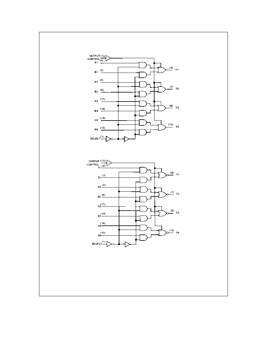
Logic Diagrams
LS257B
TL F 6417 ≠ 3
LS258B
TL F 6417 ≠ 4
5