TL F 6423
DM74LS293
4-Bit
Binary
Counter
June 1989
DM74LS293 4-Bit Binary Counter
General Description
The 'LS293 counter is electrically and functionally identical
to the 'LS93 Only the arrangement of the terminals has
been changed for the 'LS293
Each of these monolithic counters contains four master-
slave flip-flops and additional gating to provide a divide-by-
two counter and a three-stage binary counter for which the
count cycle length is divide-by-eight
All of these counters have a gated zero reset
To use the maximum count length (four-bit binary) of these
counters the B input is connected to the Q
A
output The
input count pulses are applied to input A and the outputs are
as described in the appropriate function table
Features
Y
GND and V
CC
on Corner Pins (Pins 7 and 14
respectively)
Y
Typical power dissipation 45 mW
Y
Count frequency 42 MHz
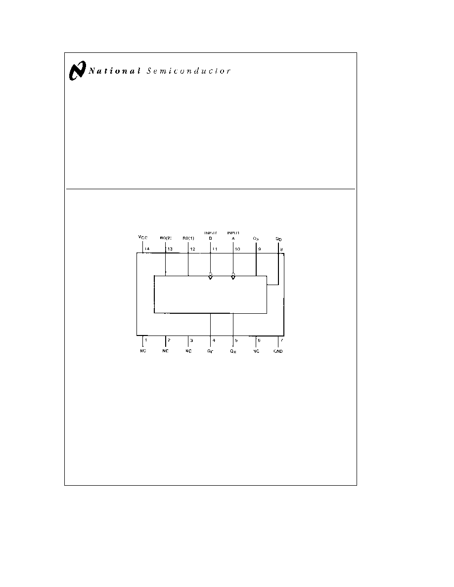
Connection Diagram
Dual-In-Line Package
TL F 6423 ≠ 1
Order Number DM74LS293M or DM74LS293N
See NS Package Number M14A or N14A
C1995 National Semiconductor Corporation
RRD-B30M105 Printed in U S A
Absolute Maximum Ratings
(Note)
If Military Aerospace specified devices are required
please contact the National Semiconductor Sales
Office Distributors for availability and specifications
Supply Voltage
7V
Input Voltage
7V
Operating Free Air Temperature Range
DM74LS
0 C to
a
70 C
Storage Temperature Range
b
65 C to
a
150 C
Note
The ``Absolute Maximum Ratings'' are those values
beyond which the safety of the device cannot be guaran-
teed The device should not be operated at these limits The
parametric values defined in the ``Electrical Characteristics''
table are not guaranteed at the absolute maximum ratings
The ``Recommended Operating Conditions'' table will define
the conditions for actual device operation
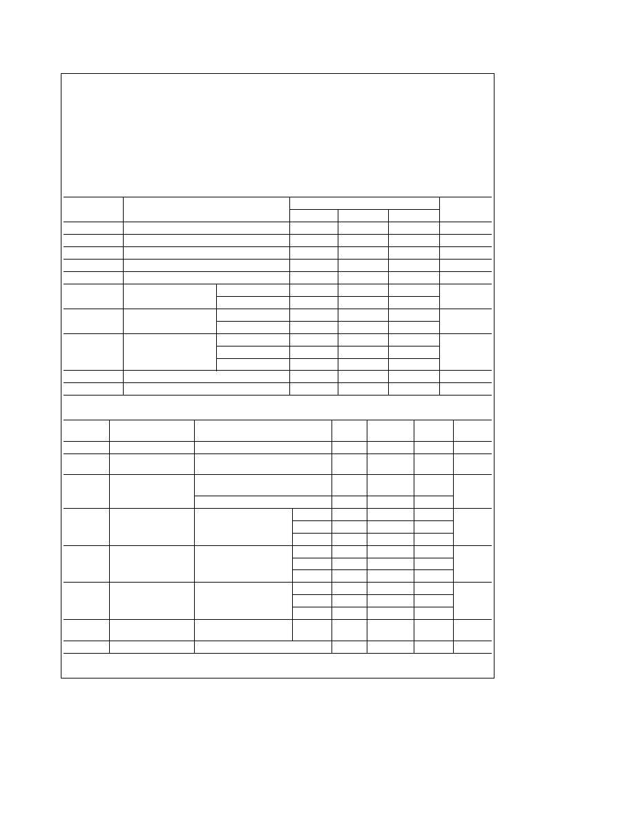
Recommended Operating Conditions
Symbol
Parameter
DM74LS293
Units
Min
Nom
Max
V
CC
Supply Voltage
4 75
5
5 25
V
V
IH
High Level Input Voltage
2
V
V
IL
Low Level Input Voltage
0 8
V
I
OH
High Level Output Current
b
0 4
mA
I
OL
Low Level Output Current
8
mA
f
CLK
Clock Frequency
A to Q
A
0
32
MHz
(Note 1)
B to Q
B
0
16
f
CLK
Clock Frequency
A to Q
A
0
20
MHz
(Note 2)
B to Q
B
0
10
t
W
Pulse Width
A
15
(Note 6)
B
30
ns
Reset
15
t
REL
Reset Release Time (Note 6)
25
ns
T
A
Free Air Operating Temperature
0
70
C
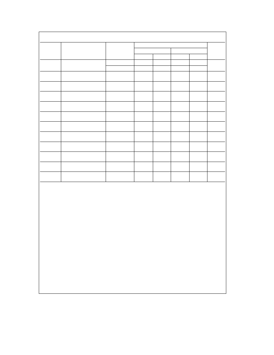
Electrical Characteristics
over recommended operating free air temperature range (unless otherwise noted)
Symbol
Parameter
Conditions
Min
Typ
Max
Units
(Note 3)
V
I
Input Clamp Voltage
V
CC
e
Min I
I
e b
18 mA
b
1 5
V
V
OH
High Level Output
V
CC
e
Min I
OH
e
Max
2 7
3 4
V
Voltage
V
IL
e
Max V
IH
e
Min
V
OL
Low Level Output
V
CC
e
Min I
OL
e
Max
0 35
0 5
V
Voltage
V
IL
e
Max V
IH
e
Min
I
OL
e
4 mA V
CC
e
Min
0 25
0 4
I
I
Input Current
Max
V
CC
e
Max
Reset
0 1
Input Voltage
V
I
e
7V
A
0 2
mA
B
0 2
I
IH
High Level Input
V
CC
e
Max
Reset
20
Current
V
I
e
2 7V
A
40
m
A
B
40
I
IL
Low Level Input
V
CC
e
Max
Reset
b
0 4
Current
V
I
e
0 4V
A
b
2 4
mA
B
b
1 6
I
OS
Short Circuit
V
CC
e
Max
b
20
b
100
mA
Output Current
(Note 4)
I
CC
Supply Current
V
CC
e
Max (Note 5)
9
15
mA
2
Switching Characteristics
at V
CC
e
5V and T
A
e
25 C (See Section 1 for Test Waveforms and Output Load)
From (Input)
R
L
e
2 kX
Symbol
Parameter
To (Output)
C
L
e
15 pF
C
L
e
50 pF
Units
Min
Max
Min
Max
t
MAX
Maximum Clock
A to Q
A
32
20
MHz
Frequency
B to Q
B
16
10
t
PLH
Propagation Delay Time
A to Q
A
16
23
ns
Low to High Level Output
t
PHL
Propagation Delay Time
A to Q
A
18
30
ns
High to Low Level Output
t
PLH
Propagation Delay Time
A to Q
D
70
87
ns
Low to High Level Output
t
PHL
Propagation Delay Time
A to Q
D
70
93
ns
High to Low Level Output
t
PLH
Propagation Delay Time
B to Q
B
16
23
ns
Low to High Level Output
t
PHL
Propagation Delay Time
B to Q
B
21
35
ns
High to Low Level Output
t
PLH
Propagation Delay Time
B to Q
C
32
48
ns
Low to High Level Output
t
PHL
Propagation Delay Time
B to Q
C
35
53
ns
High to Low Level Output
t
PLH
Propagation Delay Time
B to Q
D
51
71
ns
Low to High Level Output
t
PHL
Propagation Delay Time
B to Q
D
51
71
ns
High to Low Level Output
t
PHL
Propagation Delay Time
SET-0 to
40
53
ns
High to Low Level Output
Any Q
Note 1
C
L
e
15 pF R
L
e
2 kX T
A
e
25 C and V
CC
e
5V
Note 2
C
L
e
50 pF R
L
e
2 kX T
A
e
25 C and V
CC
e
5V
Note 3
All typicals are at V
CC
e
5V T
A
e
25 C
Note 4
Not more than one output should be shorted at a time and the duration should not exceed one second
Note 5
I
CC
is measured with all outputs open both RO inputs grounded following momentary connection to 4 5V and all other inputs grounded
Note 6
T
A
e
25 C and V
CC
e
5V
3
Function Tables
Count Sequence (See Note C)
Count
Outputs
Q
D
Q
C
Q
B
Q
A
0
L
L
L
L
1
L
L
L
H
2
L
L
H
L
3
L
L
H
H
4
L
H
L
L
5
L
H
L
H
6
L
H
H
L
7
L
H
H
H
8
H
L
L
L
9
H
L
L
H
10
H
L
H
L
11
H
L
H
H
12
H
H
L
L
13
H
H
L
H
14
H
H
H
L
15
H
H
H
H
Note C
Output Q
A
is connected to input B
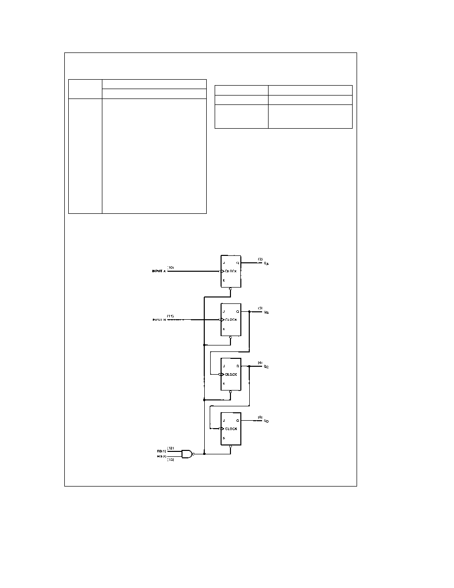
Reset Count Truth Table
Reset Inputs
Outputs
R0(1)
R0(2)
Q
D
Q
C
Q
B
Q
A
H
H
L
L
L
L
L
X
COUNT
X
L
COUNT
H
e
High Level L
e
Low Level X
e
Don't Care
Logic Diagram
LS293
TL F 6423 ≠ 2
Note
The J and K inputs shown without connection are for reference only and are functionally at a high level
4

Physical Dimensions
inches (millimeters)
14-Lead Small Outline Molded Package (M)
Order Number DM74LS293M
NS Package Number M14A
5