TL F 6428
DM54LS366ADM74LS366A
Hex
TRI-STATE
Inverting
Buffer
September 1991
DM54LS366A DM74LS366A
Hex TRI-STATE
Inverting Buffer
General Description
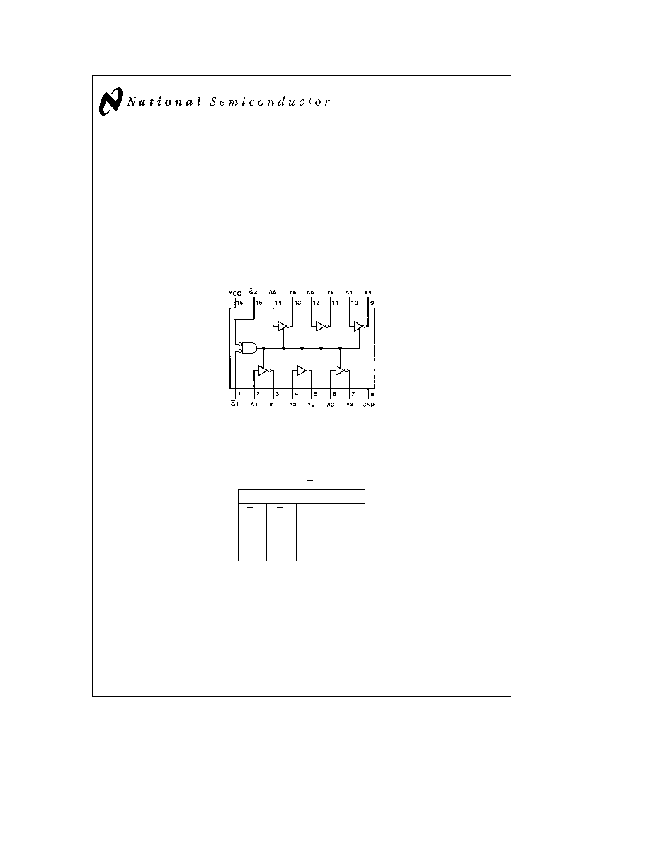
This device contains six independent gates each of which
performs an inverting buffer function The outputs have the
TRI-STATE feature When enabled the outputs exhibit the
low impedance characteristics of a standard LS output with
additional drive capability to permit the driving of bus lines
without external resistors When disabled both the output
transistors are turned off presenting a high-impedance state
to the bus line Thus the output will act neither as a signifi-
cant load nor as a driver To minimize the possibility that two
outputs will attempt to take a common bus to opposite logic
levels the disable time is shorter than the enable time of the
outputs
Connection Diagram
Dual-In-Line Package
TL F 6428 ≠ 1
Order Number DM54LS366AJ DM54LS366AW
DM54LS366AE DM74LS366AM or DM74LS366AN
See NS Package Number E20A J16A M16A N16E or W16A
Function Table
Y
e
A
Inputs
Output
G1
G2
A
Y
H
X
X
Hi-Z
X
H
X
Hi-Z
L
L
L
H
L
L
H
L
H
e
High Logic Level
L
e
Low Logic Level
X
e
Either Low or High Logic Level
Hi-Z
e
TRI-STATE (Outputs are disabled)
TRI-STATE
is a registered trademark of National Semiconductor Corporation
C1995 National Semiconductor Corporation
RRD-B30M105 Printed in U S A
Absolute Maximum Ratings
(Note)
If Military Aerospace specified devices are required
please contact the National Semiconductor Sales
Office Distributors for availability and specifications
Supply Voltage
7V
Input Voltage
7V
Operating Free Air Temperature Range
DM54LS
b
55 C to
a
125 C
DM74LS
0 C to
a
70 C
Storage Temperature Range
b
65 C to
a
150 C
Note
The ``Absolute Maximum Ratings'' are those values
beyond which the safety of the device cannot be guaran-
teed The device should not be operated at these limits The
parametric values defined in the ``Electrical Characteristics''
table are not guaranteed at the absolute maximum ratings
The ``Recommended Operating Conditions'' table will define
the conditions for actual device operation
Recommended Operating Conditions
Symbol
Parameter
DM54LS366A
DM74LS366A
Units
Min
Nom
Max
Min
Nom
Max
V
CC
Supply Voltage
4 5
5
5 5
4 75
5
5 25
V
V
IH
High Level Input Voltage
2
2
V
V
IL
Low Level Input Voltage
0 7
0 8
V
I
OH
High Level Output Current
b
1
b
2 6
mA
I
OL
Low Level Output Current
12
24
mA
T
A
Free Air Operating Temperature
b
55
125
0
70
C
Electrical Characteristics
over recommended operating free air temperature range (unless otherwise noted)
Symbol
Parameter
Conditions
Min
Typ
Max
Units
(Note 1)
V
I
Input Clamp Voltage
V
CC
e
Min I
I
e b
18 mA
b
1 5
V
V
OH
High Level Output
V
CC
e
Min I
OH
e
Max
2 4
3 4
V
Voltage
V
IL
e
Max V
IH
e
Min
V
OL
Low Level Output
V
CC
e
Min I
OL
e
Max
DM54
0 25
0 4
Voltage
V
IL
e
Max V
IH
e
Min
DM74
0 35
0 5
V
I
OL
e
12 mA V
CC
e
Min
DM74
0 25
0 4
I
I
Input Current
Max
V
CC
e
Max V
I
e
7V
DM74
0 1
mA
Input Voltage
V
CC
e
Max V
I
e
10 0V
DM54
I
IH
High Level Input Current
V
CC
e
Max V
I
e
2 7V
20
m
A
I
IL
Low Level Input
V
CC
e
Max V
I
e
0 5V
A Input
b
20
m
A
Current
(Note 4)
V
CC
e
Max V
I
e
0 4V
A Input
b
0 4
(Note 5)
mA
V
CC
e
Max V
I
e
0 4V
G Input
b
0 4
I
OZH
Off-State Output Current
V
CC
e
Max V
O
e
2 4V
with High Level Output
V
IH
e
Min V
IL
e
Max
20
m
A
Voltage Applied
I
OZL
Off-State Output Current
V
CC
e
Max V
O
e
0 4V
with Low Level Output
V
IH
e
Min V
IL
e
Max
b
20
m
A
Voltage Applied
I
OS
Short Circuit
V
CC
e
Max
DM54
b
30
b
130
mA
Output Current
(Note 2)
DM74
b
20
b
100
I
CC
Supply Current
V
CC
e
Max (Note 3)
12
21
mA
Note 1
All typicals are at V
CC
e
5V T
A
e
25 C
Note 2
Not more than one output should be shorted at a time and the duration should not exceed one second
Note 3
I
CC
is measured with the DATA inputs grounded and the OUTPUT CONTROLS at 4 5V
Note 4
Both G inputs are at 2V
Note 5
Both G inputs at 0 4V
2
Switching Characteristics
DM54LS
DM74LS
Symbol
Parameter
C
L
e
50 pF
R
L
e
667X
Units
C
L
e
50 pF
C
L
e
150 pF
Min
Max
Min
Max
Min
Max
t
PLH
Propagation Delay Time Low
12
15
25
ns
to High Level Output
t
PHL
Propagation Delay Time High
22
16
25
ns
to Low Level Output
t
PZH
Output Enable Time to
24
30
35
ns
High Level Output
t
PZL
Output Enable Time to
30
30
40
ns
Low Level Output
t
PHZ
Output Disable Time from
25
20
ns
High Level Output (Note 6)
t
PLZ
Output Disable Time from
20
20
ns
Low Level Output (Note 6)
Note 6
C
L
e
5 pF
3
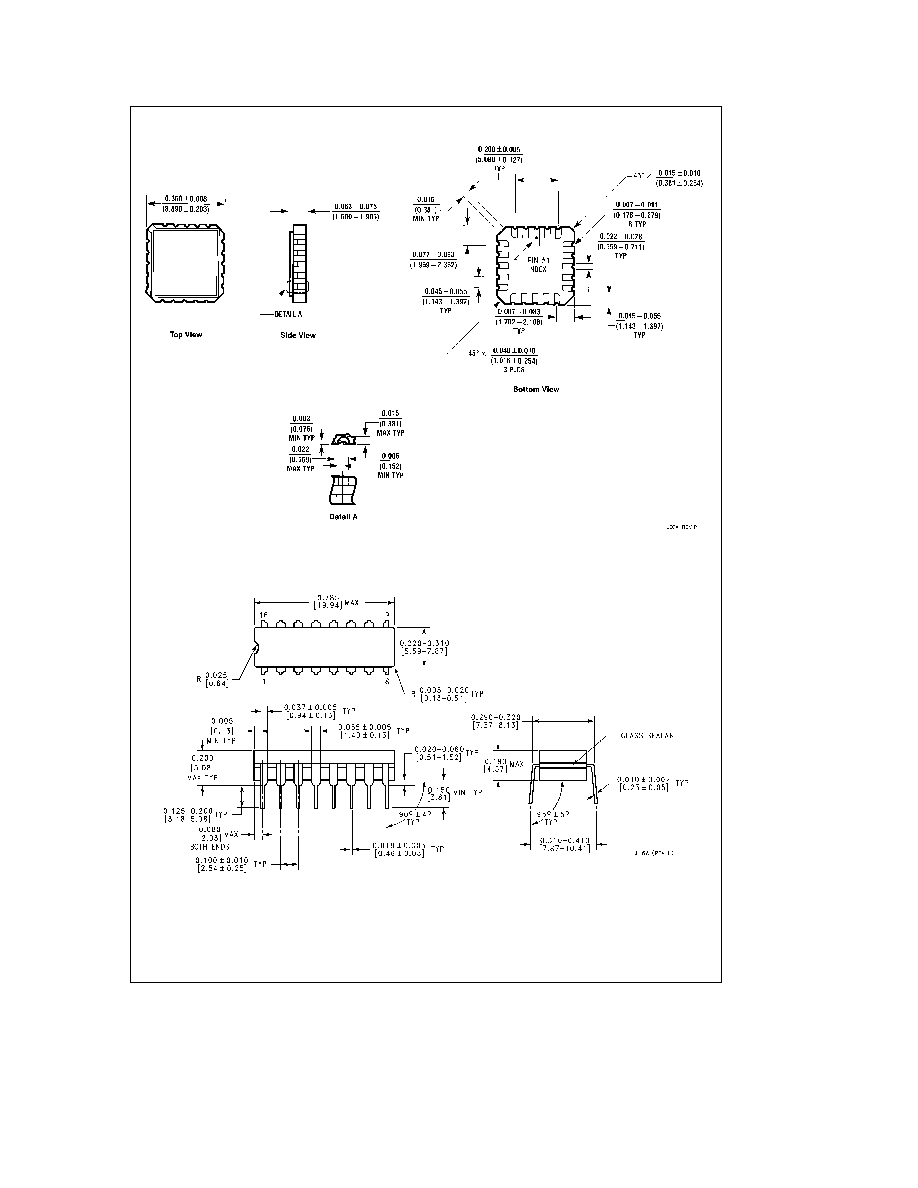
Physical Dimensions
inches (millimeters)
Ceramic Leadless Chip Carrier Package (E)
Order Number DM54LS366AE
NS Package Number E20A
16-Lead Ceramic Dual-In-Line Package (J)
Order Number DM54LS366AJ
NS Package Number J16A
4
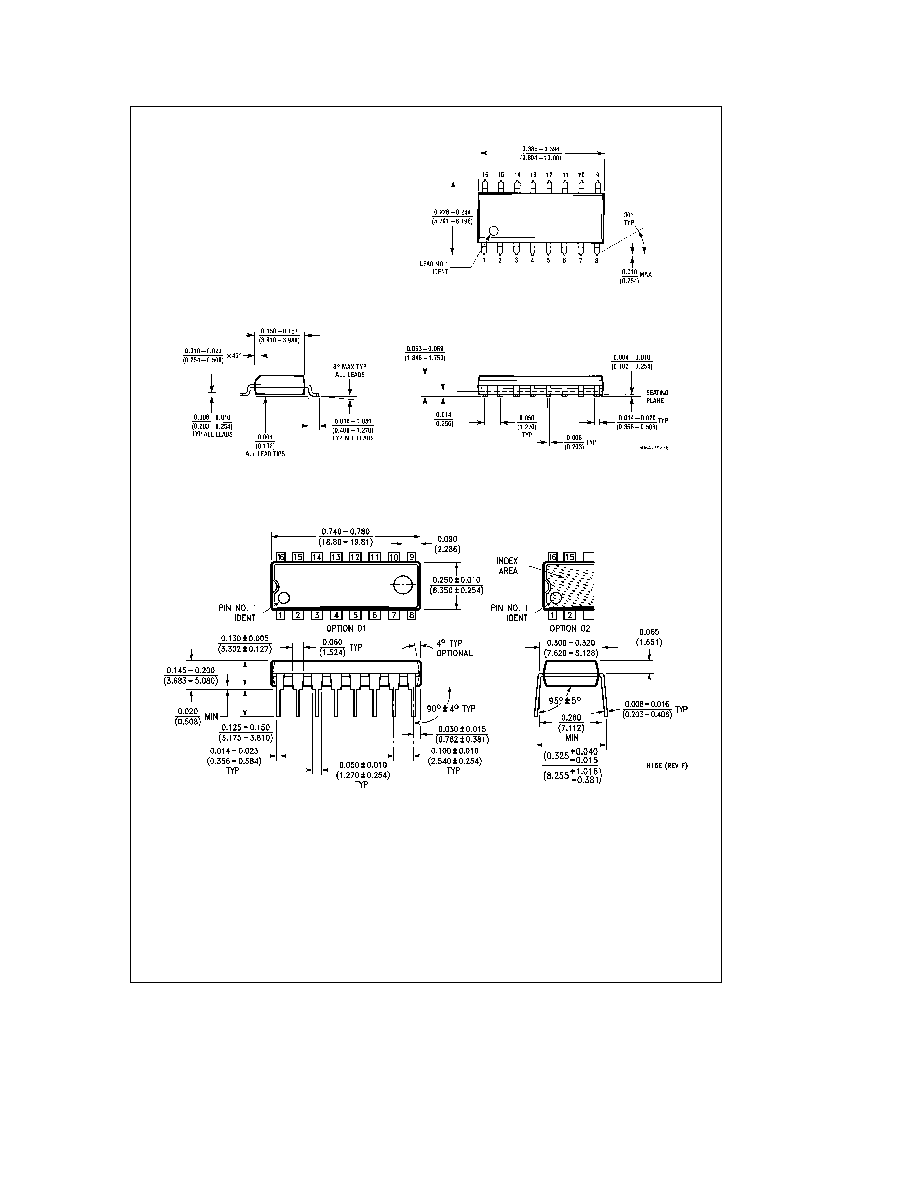
Physical Dimensions
inches (millimeters) (Continued)
16-Lead Small Outline Molded Package (M)
Order Number DM74LS366AM
NS Package Number M16A
16-Lead Molded Dual-In-Line Package (N)
Order Number DM74LS366AN
NS Package Number N16E
5