TL F 9833
DM74LS395
4-Bit
Shift
Register
with
TRI-STATE
Outputs
February 1992
DM74LS395
4-Bit Shift Register with TRI-STATE
Outputs
General Description
The LS395 is a 4-bit shift register with TRI-STATE outputs
and can operate in either a synchronous parallel load or a
serial shift-right mode as determined by the Select input An
asynchronous active LOW Master Reset (MR) input over-
rides the synchronous operations and clears the register
An active LOW Output Enable (OE) input controls the TRI-
STATE output buffers but does not interfere with the other
operations The fourth stage also has a conventional output
for linking purposes in multi-stage serial operations
Features
Y
Shift right or parallel 4-bit register
Y
TRI-STATE outputs
Y
Input clamp diodes limit high speed termination effects
Y
Fully CMOS and TTL compatible
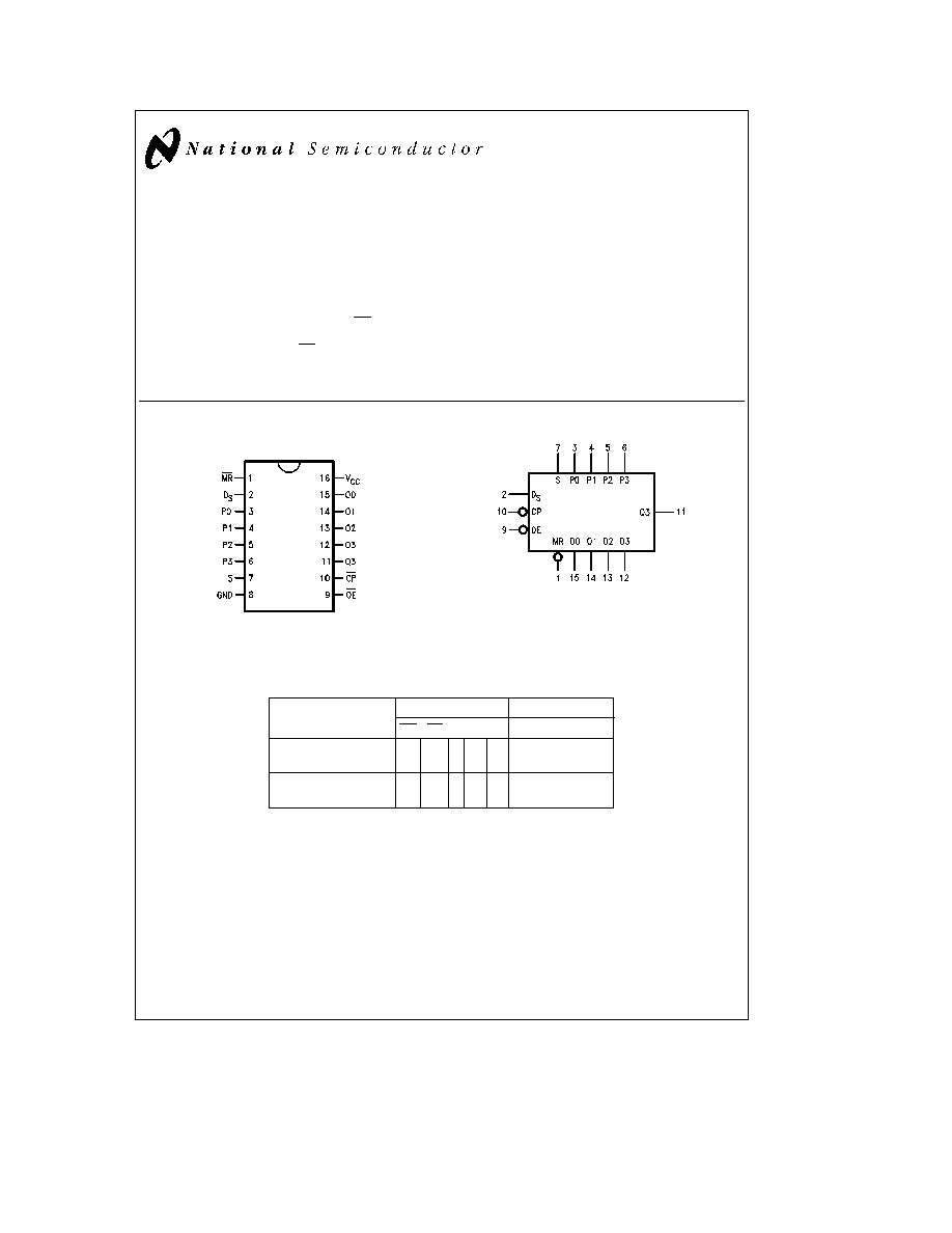
Connection Diagram
Dual-In-Line Package
TL F 9833 ≠ 1
Order Number DM74LS395WM or DM74LS395N
See NS Package Number M16B or N16E
Logic Symbol
TL F 9833 ≠ 2
V
CC
e
Pin 16
GND
e
Pin 8
Mode Select Table
Operating Mode
Inputs
t
n
Outputs
t
na1
MR
CP
S D
S
P
n
O0
O1
O2
O3
Asynchronous Reset
L
X
X
X
X
L
L
L
L
Shift SET First Stage
H
K L H
X
H
O0
n
O1
n
02
n
Shift RESET First Stage
H
K L L
X
L
O0
n
O1
n
02
n
Parallel Load
H
K H X Pn P0 P1
P2
P3
t
n
t
n
a
1
e
Time before and after CP HIGH-to-LOW transition
H
e
HIGH Voltage Level
L
e
LOW Voltage Level
X
e
Immaterial
TRI-STATE
is a registered trademark of National Semiconductor Corporation
C1995 National Semiconductor Corporation
RRD-B30M115 Printed in U S A
Absolute Maximum Ratings
(Note)
Supply Voltage
7V
Input Voltage
7V
Operating Free Air Temperature Range
0 C to
a
70 C
Storage Temperature Range
b
65 C to
a
150 C
Note
The ``Absolute Maximum Ratings'' are those values
beyond which the safety of the device cannot be guaran-
teed The device should not be operated at these limits The
parametric values defined in the ``Electrical Characteristics''
table are not guaranteed at the absolute maximum ratings
The ``Recommended Operating Conditions'' table will define
the conditions for actual device operation
Recommended Operating Conditions
Symbol
Parameter
Min
Nom
Max
Units
V
CC
Supply Voltage
4 75
5
5 25
V
V
IH
High Level Input Voltage
2
V
V
IL
Low Level Input Voltage
0 8
V
I
OH
High Level Output Current
b
0 4
mA
I
OL
Low Level Output Current
8
mA
T
A
Free Air Operating Temperature
0
70
C
t
s
(H)
Setup Time HIGH or LOW
20
ns
t
s
(L)
S D
S
or P
n
to CP
20
t
h
(H)
Hold Time HIGH or LOW
5
ns
t
h
(L)
S D
S
or P
n
to CP
5
t
w
(L)
CP Pulse Width LOW
18
ns
t
w
(L)
MR Pulse Width LOW
20
ns
Electrical Characteristics
Over recommended operating free air temperature range (unless otherwise noted)
Symbol
Parameter
Conditions
Min
Typ
Max
Units
(Note 1)
V
I
Input Clamp Voltage
V
CC
e
Min I
I
e b
18 mA
b
1 5
V
V
OH
High Level Output
V
CC
e
Min I
OH
e
Max
2 7
V
Voltage
V
IL
e
Max
V
OL
Low Level Output
V
CC
e
Min I
OL
e
Max
0 35
0 5
Voltage
V
IH
e
Min
V
I
OL
e
4 mA V
CC
e
Min
0 25
0 4
I
I
Input Current
Max
V
CC
e
Max V
I
e
7V
0 1
mA
Input Voltage
I
IH
High Level Input Current
V
CC
e
Max V
I
e
2 7V
20
m
A
I
IL
Low Level Input Current
V
CC
e
Max V
I
e
0 4V
b
0 4
mA
I
OS
Short Circuit Output Current
V
CC
e
Max (Note 2)
b
20
b
100
mA
I
CC
Supply Current with
V
CC
e
Max OE D
S
S
e
4 5V
29
mA
Outputs OFF
CP
e
K P
n
e
GND
Supply Current with
V
CC
e
Max D
S
S
e
4 5V
25
mA
Outputs ON
OE CP P
n
e
GND
I
OZH
TRI-STATE Output Off
V
CC
e
V
CCH
20
m
A
Current HIGH
V
OZH
e
2 7V
I
OZL
TRI-STATE Output Off
V
CC
e
V
CCH
b
20
m
A
Current LOW
V
OZL
e
0 4V
Note 1
All typicals are at V
CC
e
5V T
A
e
25 C
Note 2
Not more than one output should be shorted at a time and the duration should not exceed one second
2
Switching Characteristics
V
CC
e a
5 0V T
A
e a
25 C
Symbol
Parameter
R
L
e
2 kX C
L
e
15 pF
Units
Min
Max
f
max
Maximum Shift Frequency
30
MHz
t
PLH
Propagation Delay
35
ns
t
PHL
CP to O
n
25
t
PHL
Propagation Delay
35
ns
MR to O
n
t
PZH
Output Enable Time
20
ns
t
PZL
20
t
PHZ
Output Disable Time
17
ns
t
PLZ
23
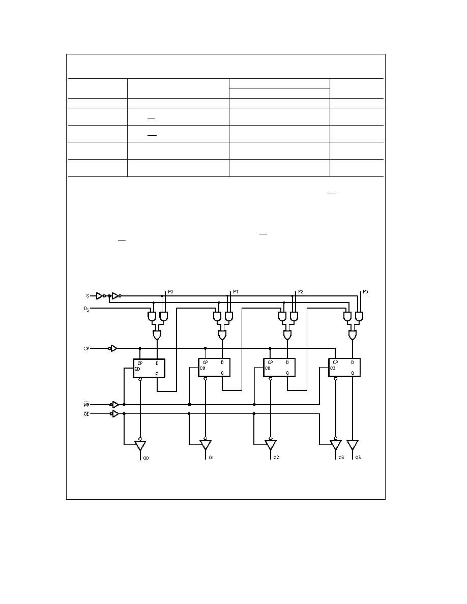
Functional Description
The `LS395 contains four D-type edge-triggered flip-flops
and auxiliary gating to select a D input either from a Parallel
(P
n
) input or from the preceding stage When the Select
input is HIGH the P
n
inputs are enabled A LOW signal in
the S input enables the serial inputs for shift-right opera-
tions as indicated in the Truth Table
State changes are initiated by HIGH-to-LOW transitions on
the Clock Pulse (CP) input Signals on the P
n
D
S
and S
inputs can change when the Clock is in either state provid-
ed that the recommended setup and hold times are ob-
served When the S input is LOW a CP HIGH-LOW tran-
sition transfers data in O0 to O1 O1 to O2 and O2 to O3 A
left-shift is accomplished by connecting the outputs back to
the P
n
inputs but offset one place to the left i e O3 to P2
O2 to P1 and O1 to P0 with P3 acting as the linking input
from another package
When the OE input is HIGH the output buffers are disabled
and the O0 ≠ O3 outputs are in a high impedance condition
The shifting parallel loading or resetting operations can still
be accomplished however
Logic Diagram
TL F 9833 ≠ 3
3

4
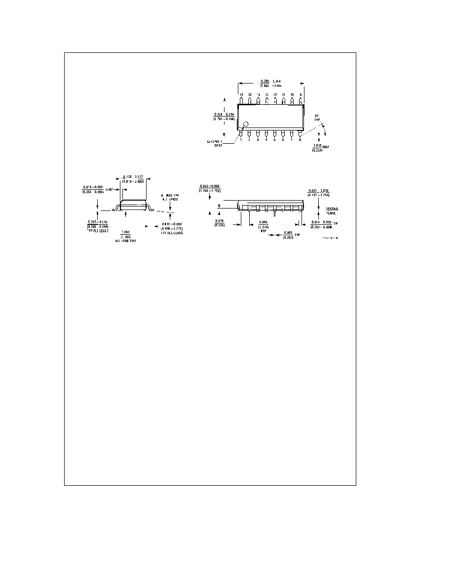
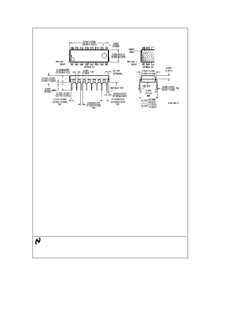
Physical Dimensions
inches (millimeters)
16-Lead Wide Small Outline Molded Package (M)
Order Number DM74LS395WM
NS Package Number M16B
5
DM74LS395
4-Bit
Shift
Register
with
TRI-STATE
Outputs
Physical Dimensions
inches (millimeters) (Continued)
16-Lead Molded Dual-In-Line Package (N)
Order Number DM74LS395N
NS Package Number N16E
LIFE SUPPORT POLICY
NATIONAL'S PRODUCTS ARE NOT AUTHORIZED FOR USE AS CRITICAL COMPONENTS IN LIFE SUPPORT
DEVICES OR SYSTEMS WITHOUT THE EXPRESS WRITTEN APPROVAL OF THE PRESIDENT OF NATIONAL
SEMICONDUCTOR CORPORATION As used herein
1 Life support devices or systems are devices or
2 A critical component is any component of a life
systems which (a) are intended for surgical implant
support device or system whose failure to perform can
into the body or (b) support or sustain life and whose
be reasonably expected to cause the failure of the life
failure to perform when properly used in accordance
support device or system or to affect its safety or
with instructions for use provided in the labeling can
effectiveness
be reasonably expected to result in a significant injury
to the user
National Semiconductor
National Semiconductor
National Semiconductor
National Semiconductor
Corporation
Europe
Hong Kong Ltd
Japan Ltd
1111 West Bardin Road
Fax (a49) 0-180-530 85 86
13th Floor Straight Block
Tel 81-043-299-2309
Arlington TX 76017
Email cnjwge tevm2 nsc com
Ocean Centre 5 Canton Rd
Fax 81-043-299-2408
Tel 1(800) 272-9959
Deutsch Tel (a49) 0-180-530 85 85
Tsimshatsui Kowloon
Fax 1(800) 737-7018
English
Tel (a49) 0-180-532 78 32
Hong Kong
Fran ais Tel (a49) 0-180-532 93 58
Tel (852) 2737-1600
Italiano
Tel (a49) 0-180-534 16 80
Fax (852) 2736-9960
National does not assume any responsibility for use of any circuitry described no circuit patent licenses are implied and National reserves the right at any time without notice to change said circuitry and specifications