Äîêóìåíòàöèÿ è îïèñàíèÿ www.docs.chipfind.ru
TL L 8334
DM54LS461DM74LS461
Octal
Counter
July 1989
DM54LS461 DM74LS461 Octal Counter
General Description
The LS461 is an 8-bit synchronous counter with parallel
load clear and hold capability Two function select inputs
(I
0
I
1
) provide one of four operations which occur synchro-
nously on the rising edge of the clock (CK)
The LOAD operation loads the inputs (D
7
D
0
) into the out-
put register (Q
7
Q
0
) The CLEAR operation resets the out-
put register to all LOWs The HOLD operation holds the
previous value regardless of clock transitions The INCRE-
MENT operation adds one to the output register when the
carry-in input is TRUE (CI
e
LOW) otherwise the operation
is a HOLD The carry-out (CO) is TRUE (CO
e
LOW) when
the output register (Q
7
Q
0
) is all HIGHs otherwise FALSE
(CO
e
HIGH)
The output register (Q
7
Q
0
) is enabled when OE is LOW
and disabled (HI-Z) when OE is HIGH The output drivers
will sink the 24 mA required for many bus interface stand-
ards
Two or more LS461 octal counters may be cascaded to
provide larger counters The operation codes were chosen
such that when I
1
is HIGH I
0
may be used to select be-
tween LOAD and INCREMENT as in a program counter
(JUMP INCREMENT)
Features Benefits
Y
Octal counter for microprogram-counter DMA controller
and general purpose counting applications
Y
8 bits match byte boundaries
Y
Bus-structured pinout
Y
24-pin Skinny Dip saves space
Y
TRI-STATE
outputs drive bus lines
Y
Low current PNP inputs reduce loading
Y
Expandable in 8-bit increments
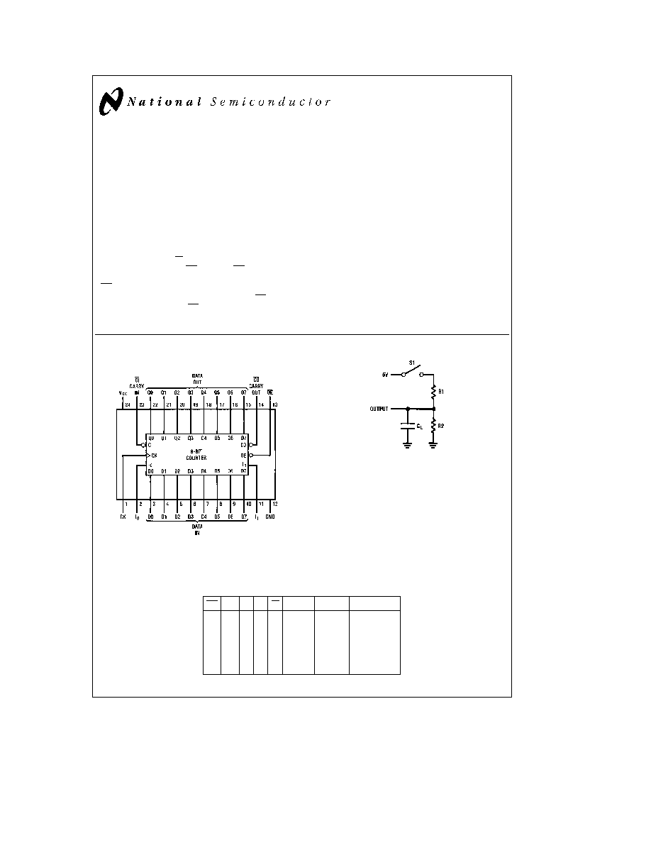
Connection Diagram
Top View
TL L 8334 1
Order Number DM54LS461J
DM74LS461J or DM74LS461N
See NS Package Number J24F or N24C
Standard Test Load
TL L 8334 2
Function Table
OE
CK
I1
I0
CI
D7 D0
Q7 Q0
Operation
H
X
X
X
X
X
Z
HI-Z
L
u
L
L
X
X
L
CLEAR
L
u
L
H
X
X
Q
HOLD
L
u
H
L
X
D
D
LOAD
L
u
H
H
H
X
Q
HOLD
L
u
H
H
L
X
Q plus 1
INCREMENT
TRI-STATE
is a registered trademark of National Semiconductor Corp
C1995 National Semiconductor Corporation
RRD-B30M115 Printed in U S A
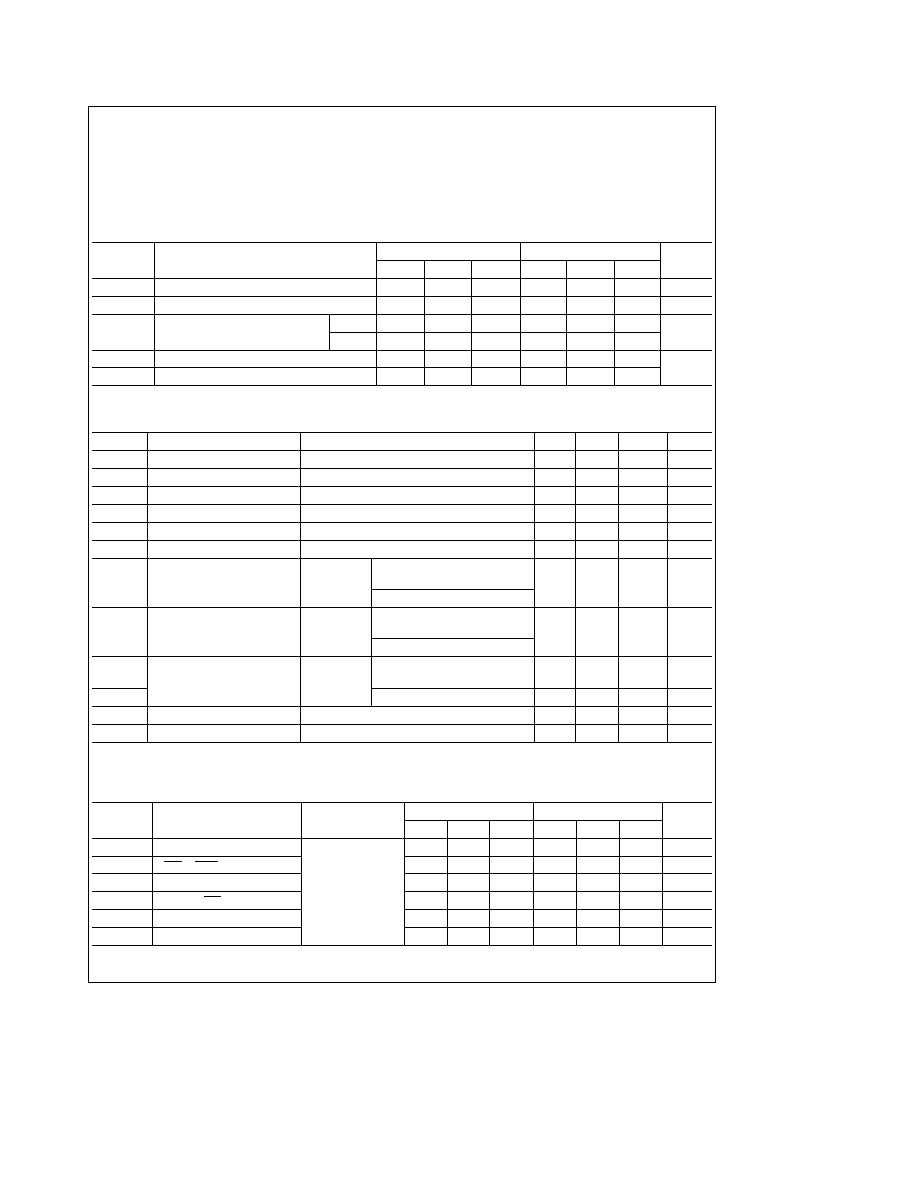
Absolute Maximum Ratings
If Military Aerospace specified devices are required
please contact the National Semiconductor Sales
Office Distributors for availability and specifications
Supply Voltage V
CC
7V
Input Voltage
5 5V
Off-State Output Voltage
5 5V
Storage Temperature
b
65 C to
a
150 C
Operating Conditions
Symbol
Parameter
Military
Commercial
Units
Min
Typ
Max
Min
Typ
Max
V
CC
Supply Voltage
4 5
5
5 5
4 75
5
5 25
V
T
A
Operating Free-Air Temperature
b
55
125
0
75
C
t
W
Width of Clock
Low
40
35
ns
High
30
25
t
SU
Set Up Time
60
50
ns
t
h
Hold Time
0
b
15
0
b
15
Case Temperature
Electrical Characteristics
Over Operating Conditions
Symbol
Parameter
Test Conditions
Min
Typ
Max
Units
V
IL
Low-Level Input Voltage
0 8
V
V
IH
High-Level Input Voltage
2
V
V
IC
Input Clamp Voltage
V
CC
e
MIN
I
I
e b
18 mA
b
1 5
V
I
IL
Low-Level Input Current
V
CC
e
MAX
V
I
e
0 4V
b
0 25
mA
I
IH
High-Level Input Current
V
CC
e
MAX
V
I
e
2 4V
25
m
A
I
I
Maximum Input Current
V
CC
e
MAX
V
I
e
5 5V
1
mA
V
CC
e
MIN
MIL
I
OL
e
12 mA
V
OL
Low-Level Output Voltage
V
IL
e
0 8V
0 5
V
V
IH
e
2V
COM
I
OL
e
24 mA
V
CC
e
MIN
MIL
I
OH
e b
2 mA
V
OH
High-Level Output Voltage
V
IL
e
0 8V
2 4
V
V
IH
e
2V
COM
I
OH
e b
3 2 mA
V
CC
e
MAX
V
O
e
0 4V
b
100
m
A
I
OZL
Off-State Output Current
V
IL
e
0 8V
I
OZH
V
IH
e
2V
V
O
e
2 4V
100
m
A
I
OS
Output Short-Circuit Current
V
CC
e
5 0V
V
CC
e
0V
b
30
b
130
mA
I
CC
Supply Current
V
CC
e
MAX
120
180
mA
No more than one output should be shorted at a time and duration of the short-circuit should not exceed one second
All typical values are at V
CC
e
5V T
A
e
25 C
Switching Characteristics
Over Operating Conditions
Symbol
Parameter
Test Conditions
Military
Commercial
Units
(See Test Load)
Min
Typ
Max
Min
Typ
Max
f
MAX
Maximum Clock Frequency
10 5
12 5
MHz
t
PD
CBI to CBO Delay
C
L
e
50 pF
35
60
35
50
ns
t
PD
Clock to Q
R
1
e
200 X
20
35
20
30
ns
t
PD
Clock to CO
R
2
e
390 X
55
95
55
80
ns
t
PZX
Output Enable Delay
35
55
35
45
ns
t
PXZ
Output Disable Delay
35
55
35
45
ns
2
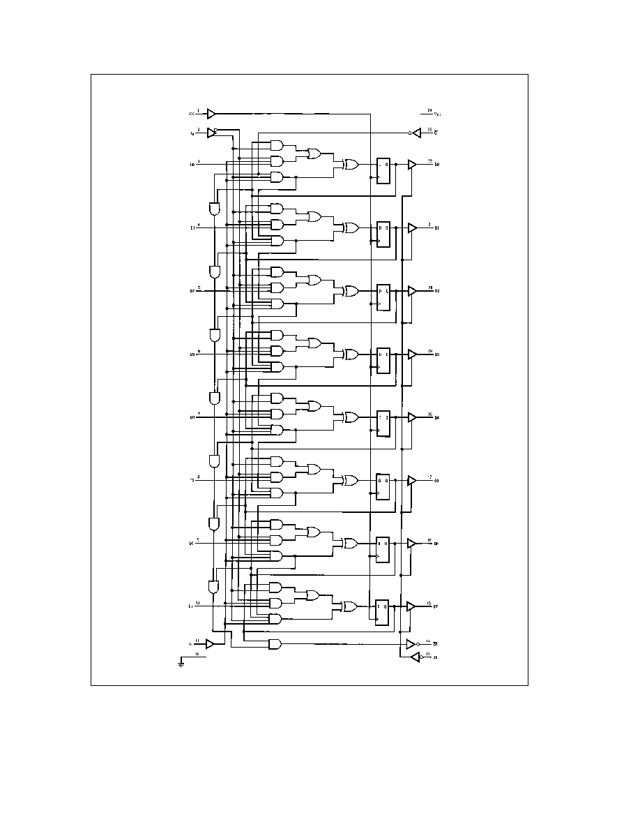
Logic Diagram
LS461
TL L 8334 3
3
DM54LS461DM74LS461
Octal
Counter
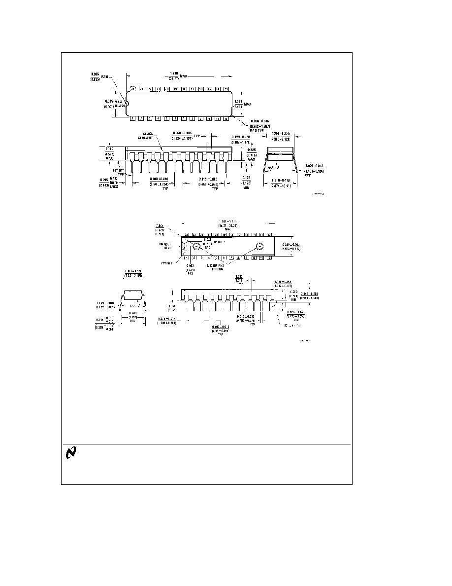
Physical Dimensions
inches (millimeters)
24-Pin Narrow Ceramic Dual-In-Line Package (J)
Order Number DM54LS461J or DM74LS461J
NS Package J24F
24-Pin Narrow Plastic Dual-In-Line Package (N)
Order Number DM74LS461N
NS Package N24C
LIFE SUPPORT POLICY
NATIONAL'S PRODUCTS ARE NOT AUTHORIZED FOR USE AS CRITICAL COMPONENTS IN LIFE SUPPORT
DEVICES OR SYSTEMS WITHOUT THE EXPRESS WRITTEN APPROVAL OF THE PRESIDENT OF NATIONAL
SEMICONDUCTOR CORPORATION As used herein
1 Life support devices or systems are devices or
2 A critical component is any component of a life
systems which (a) are intended for surgical implant
support device or system whose failure to perform can
into the body or (b) support or sustain life and whose
be reasonably expected to cause the failure of the life
failure to perform when properly used in accordance
support device or system or to affect its safety or
with instructions for use provided in the labeling can
effectiveness
be reasonably expected to result in a significant injury
to the user
National Semiconductor
National Semiconductor
National Semiconductor
National Semiconductor
Corporation
Europe
Hong Kong Ltd
Japan Ltd
1111 West Bardin Road
Fax (a49) 0-180-530 85 86
13th Floor Straight Block
Tel 81-043-299-2309
Arlington TX 76017
Email cnjwge tevm2 nsc com
Ocean Centre 5 Canton Rd
Fax 81-043-299-2408
Tel 1(800) 272-9959
Deutsch Tel (a49) 0-180-530 85 85
Tsimshatsui Kowloon
Fax 1(800) 737-7018
English
Tel (a49) 0-180-532 78 32
Hong Kong
Fran ais Tel (a49) 0-180-532 93 58
Tel (852) 2737-1600
Italiano
Tel (a49) 0-180-534 16 80
Fax (852) 2736-9960
National does not assume any responsibility for use of any circuitry described no circuit patent licenses are implied and National reserves the right at any time without notice to change said circuitry and specifications