TL F 10174
DM54LS55DM74LS55
2-Wide
4-Input
AND-OR-INVERT
Gate
April 1992
DM54LS55 DM74LS55
2-Wide 4-Input AND-OR-INVERT Gate
General Description
This device contains a combination of AND-OR-INVERT
functions
The internal gates are configured as two
four-input AND gates with their outputs connected to a
two-input NOR gate
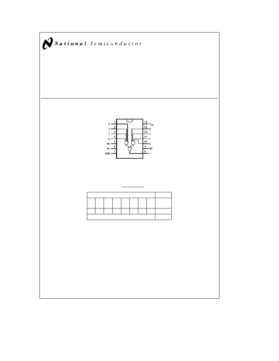
Connection Diagram
Dual-In-Line Package
TL F 10174 ≠ 1
Order Number DM54LS55J DM54LS55W DM74LS55M or DM74LS55N
See NS Package Number J14A M14A N14A or W14B
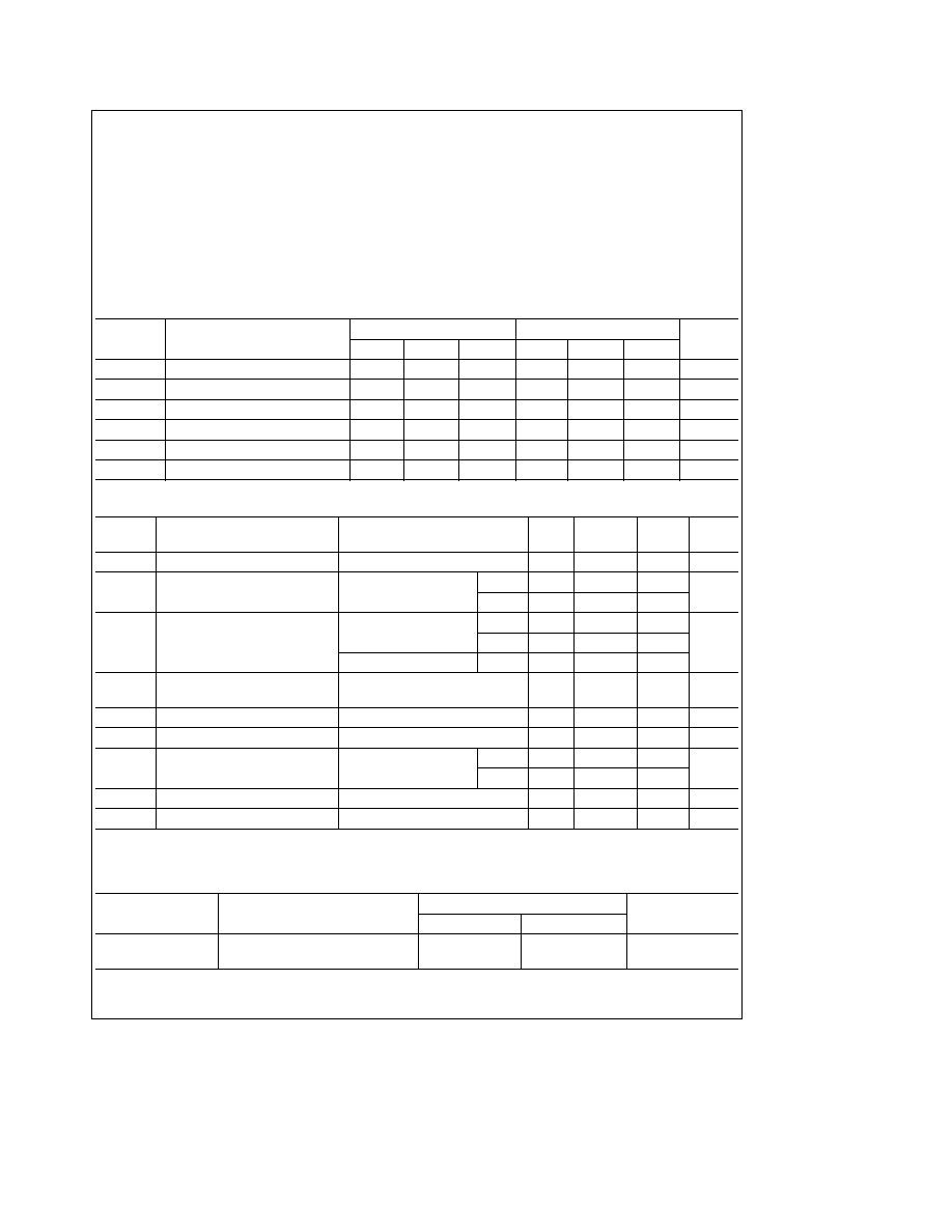
Function Table
Y
e
ABCD
a
EFGH
Inputs
Output
A
B
C
D
E
F
G
H
Y
H
H
H
H
X
X
X
X
L
X
X
X
X
H
H
H
H
L
All Other Combinations
H
H
e
High Logic Level
L
e
Low Logic Level
X
e
Either Low or High Logic Level
C1995 National Semiconductor Corporation
RRD-B30M105 Printed in U S A
Absolute Maximum Ratings
(Note)
If Military Aerospace specified devices are required
please contact the National Semiconductor Sales
Office Distributors for availability and specifications
Supply Voltage
7V
Input Voltage
7V
Operating Free Air Temperature Range
DM54LS
b
55 C to
a
125 C
DM74LS
0 C to
a
70 C
Storage Temperature Range
b
65 C to
a
150 C
Note
The ``Absolute Maximum Ratings'' are those values
beyond which the safety of the device cannot be guaran-
teed The device should not be operated at these limits The
parametric values defined in the ``Electrical Characteristics''
table are not guaranteed at the absolute maximum ratings
The ``Recommended Operating Conditions'' table will define
the conditions for actual device operation
Recommended Operating Conditions
Symbol
Parameter
DM54LS55
DM74LS55
Units
Min
Nom
Max
Min
Nom
Max
V
CC
Supply Voltage
4 5
5
5 5
4 75
5
5 25
V
V
IH
High Level Input Voltage
2
2
V
V
IL
Low Level Input Voltage
0 7
0 8
V
I
OH
High Level Output Current
b
0 4
b
0 4
mA
I
OL
Low Level Output Current
4
8
mA
T
A
Free Air Operating Temperature
b
55
125
0
70
C
Electrical Characteristics
over recommended operating free air temperature range (unless otherwise noted)
Symbol
Parameter
Conditions
Min
Typ
Max
Units
(Note 1)
V
I
Input Clamp Voltage
V
CC
e
Min I
I
e b
18 mA
b
1 5
V
V
OH
High Level Output Voltage
V
CC
e
Min I
OH
e
Max
DM54
2 5
V
V
IL
e
Max
DM74
2 7
V
OL
Low Level Output Voltage
V
CC
e
Min I
OL
e
Max
DM54
0 4
V
IH
e
Min
DM74
0 5
V
I
OL
e
4 mA V
CC
e
Min
DM74
0 4
I
I
Input Current
Max
V
CC
e
Max V
I
e
7V
0 1
mA
Input Voltage
V
I
e
10V (DM54)
I
IH
High Level Input Current
V
CC
e
Max V
I
e
2 7V
20
m
A
I
IL
Low Level Input Current
V
CC
e
Max V
I
e
0 4V
b
0 4
mA
I
OS
Short Circuit
V
CC
e
Max
DM54
b
20
b
100
mA
Output Current
(Note 2)
DM74
b
20
b
100
I
CCH
Supply Current with Outputs High
V
CC
e
Max V
IN
e
GND
0 8
mA
I
CCL
Supply Current with Outputs Low
V
CC
e
Max V
IN
e
Open
1 3
mA
Note 1
All typicals are at V
CC
e
5V T
A
e
25 C
Note 2
Not more than one output should be shorted at a time and the duration should not exceed one second
Switching Characteristics
V
CC
e a
5 0V T
A
e a
25 C
Symbol
Parameter
C
L
e
15 pF R
L
e
2 kX
Units
Min
Max
t
PLH
Propagation Delay Time
15
ns
t
PHL
15
2
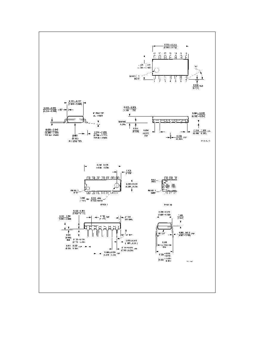
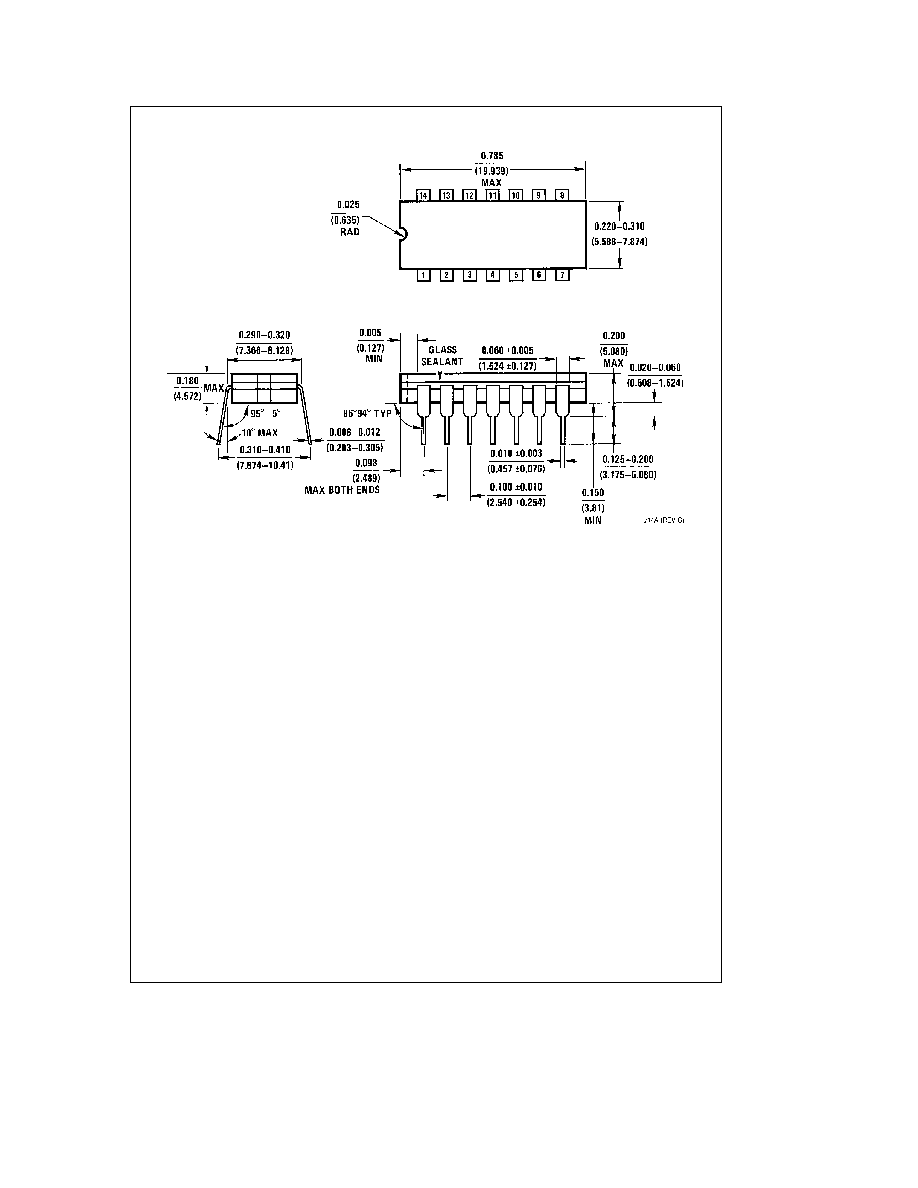
Physical Dimensions
inches (millimeters) (Continued)
14-Lead Small Outline Molded Package (M)
Order Number DM74LS55M
NS Package Number M14A
14-Lead Molded Dual-In-Line Package (N)
Order Number DM74LS55N
NS Package Number N14A
5