 | –≠–ª–µ–∫—Ç—Ä–æ–Ω–Ω—ã–π –∫–æ–º–ø–æ–Ω–µ–Ω—Ç: DM74LS962 | –°–∫–∞—á–∞—Ç—å:  PDF PDF  ZIP ZIP |
TL F 6438
DM74LS962
(DM86LS62)
Dual
Rank
8-Bit
TRI-STATE
Shift
Register
August 1991
DM74LS962 (DM86LS62)
Dual Rank 8-Bit TRI-STATE
Shift Register
General Description
These circuits are TRI-STATE edge-triggered 8-bit I O reg-
isters in parallel with 8-bit serial shift registers which are
capable of operating in any of the following modes parallel
load from I O pins to register ``A'' parallel transfer down
from register ``A'' to serial shift register ``B'' parallel transfer
up from shift register ``B'' to register ``A'' serial shift of regis-
ter ``B'' or exchange data between register ``A'' and shift
register ``B'' Since the registers are edge-triggered by the
positive transition of the clock the control lines which deter-
mine the mode or operation are completely independent of
the logic level applied to the clock Designed for bus-orient-
ed systems these circuits have their TRI-STATE inputs and
outputs on the same pins
Features
Y
Registers are edge-triggered by the positive transition
of the clock
Y
All inputs are PNP transistors
Y
Input disable dominates over output disable
Y
Output high impedance state does not impede any oth-
er mode of operation
Y
8-bit I O pins are TRI-STATE buffers
Y
Typical shift frequency is 36 MHz
Y
Typical power dissipation is 305 mW
Y
All control inputs are active when in an ``L'' logic state
Y
Devices can be cascaded into N-bit word
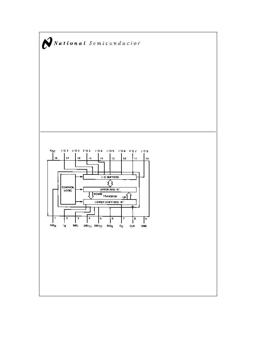
Connection Diagram
Dual-In-Line Package
TL F 6438 ≠ 1
Top View
Order Number DM74LS962N or DM86LS62N
See NS Package Number N18A
Pin Description
DIS
O
Output disable
I
S
Serial input
DIS
I
Input disable
DIS
TU
Transfer up disable
DIS
TD
Transfer down disable
DIS
S
Shift disable
O
S
Serial output
CLK
Clock
GND
Ground
I O 1
I O 8
8-bit I O pins
V
CC
Supply Voltage
TRI-STATE
is a registered trademark of National Semiconductor Corporation
C1995 National Semiconductor Corporation
RRD-B30M105 Printed in U S A
Absolute Maximum Ratings
(Note)
Supply Voltage
7V
Input Voltage
7V
Operating Free Air Temperature Range
DM74LS DM86LS
0 C to
a
70 C
Storage Temperature Range
b
65 C to
a
150 C
Lead Temperature (Soldering 10 seconds)
300 C
Note
The ``Absolute Maximum Ratings'' are those values
beyond which the safety of the device cannot be guaran-
teed The device should not be operated at these limits The
parametric values defined in the ``Electrical Characteristics''
table are not guaranteed at the absolute maximum ratings
The ``Recommended Operating Conditions'' table will define
the conditions for actual device operation
Recommended Operating Conditions
Symbol
Parameter
Min
Typ
Max
Units
V
CC
Supply Voltage
4 75
5
5 25
V
V
IH
High-Level Input Voltage
2
V
V
IL
Low-Level Input Voltage
0 8
V
I
OH
High-Level Output Current
b
5 2
mA
I
OL
Low-Level Output Current
16
mA
f
CLOCK
Clock Frequency (Note 5)
0
25
MHz
Clock
High Pulse Width (Note 5)
25
17
ns
Pulse
Low Pulse Width (Note 5)
15
7
ns
t
SET-UP
Data Set-Up Time (Note 5)
10
ns
t
HOLD
Data Hold Time (Note 5)
0
ns
T
A
Free Air Operating Temperature
0
70
C
Electrical Characteristics
over recommended operating free air temperature range (unless otherwise noted)
Symbol
Parameter
Conditions (1)
Min
Typ (2)
Max
Units
V
I
Input Clamp Voltage
V
CC
e
Min I
I
e b
18 mA
b
1 5
V
V
OH
High-Level Output Voltage
V
CC
e
Min V
IH
e
2 V
I
OH
e b
2 6 mA
V
V
IL
e
V
IL
Max
I
OH
e b
5 2 mA
2 4
V
OL
Low-Level Output Voltage
V
CC
e
Min V
IH
e
2 V
I
OL
e
8 mA
0 25
0 4
V
V
IL
e
V
IL
Max
I
OL
e
16 mA
0 35
0 5
I
I
Input Current at Maximum
V
CC
e
Max V
I
e
5 5V
0 1
mA
Input Voltage
I
IH
High-Level Input Current
V
CC
e
Max V
I
e
2 7V
20
m
A
I
IL
Low-Level Input Current
V
CC
e
Max V
I
e
0 4V
b
50
m
A
I
OS
Short-Circuit Output Current
V
CC
e
Max (3)
b
20
b
100
mA
I
CC
Supply Current
V
CC
e
Max (4)
61
99
mA
I
OFF
TRI-STATE I O Current
V
CC
e
Max V
IH
e
2V
V
O
e
2 4V
20
m
A
V
O
e
0 4V
b
20
m
A
Note 1
For conditions shown as min or max use the appropriate value specified under recommended operating conditions
Note 2
All typical values are at V
CC
e
5V T
A
e
25 C
Note 3
Not more than one output should be shorted at a time and the duration of the short circuit should not exceed one second
Note 4
I
CC
is measured with serial output open the clock and shift disable input at 2 4V All other control inputs and I O pins grounded
Note 5
T
A
e
25 C and V
CC
e
5V
2

Switching Characteristics
V
CC
e
5V and T
A
e
25 C
Symbol
Parameter
Conditions
Min
Max
Units
f
MAX
Maximum Clock Frequency
25
MHz
t
PLH
Propagation Delay Time Low-to-High-Level
7
33
ns
from Clock to Any Outputs
t
PHL
Propagation Delay Time High-to-Low Level
10
48
ns
from Clock to Any Outputs
C
L
e
15 pF R
L
e
1 kX
t
ENABLE
Enable Time from Any Control Inputs
5
30
ns
t
DISABLE
Disable Time from Any Control Inputs
6
30
ns
t
ZH
Output Enable Time to High Level
5
23
ns
t
ZL
Output Enable to Low Level
4
18
ns
t
HZ
Output Disable Time from High Level
C
L
e
5 pF R
L
e
1 kX
5
23
ns
t
LZ
Output Disable Time from Low Level
6
27
ns
Logic Diagram
TL F 6438 ≠ 2
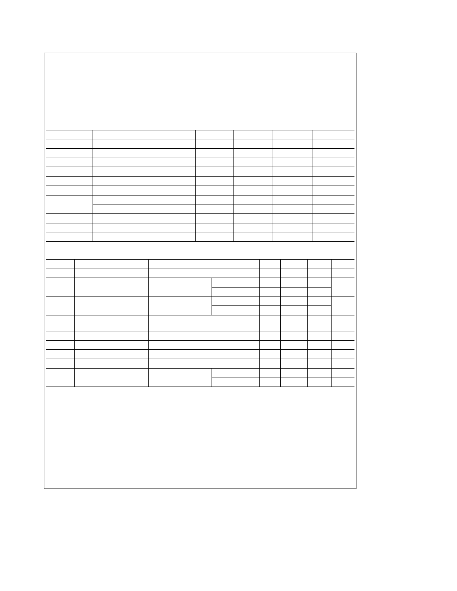
3

Function
Table
Table
I
DIS
O
DIS
I
DIS
TU
DIS
TD
DIS
S
CLK
I
S
8-Bit
IO
Content
of
Upper
Reg
``A''
Content
of
Lower
Serial
Shift
Reg
``B''
O
S
Comments
Pins
A1
A2
A3
A4
A5
A6
A7
A8
B1
B2
B3
B4
B5
B6
B7
B8
H
H
H
H
H
X
X
Hi-Z
a1
a2
a3
a4
a5
a6
a7
a8
b1
b2
b3
b4
b5
b6
b7
b8
b8
Stable
state
L
H
H
H
H
X
X
Output
a1
a2
a3
a4
a5
a6
a7
a8
b1
b2
b3
b4
b5
b6
b7
b8
b8
XL
H
H
H
u
X
Input
I
1
I
2
I
3
I
4
I
5
I
6
I
7
I
8
b1
b2
b3
b4
b5
b6
b7
b8
b8
Entering
data
from
IO
to
reg
``A''
HH
L
H
H
u
X
Hi-Z
b1
b2
b3
b4
b5
b6
b7
b8
b1
b2
b3
b4
b5
b6
b7
b8
b8
Transfer
data
up
from
reg
``B''
to
reg
``A''
LH
L
H
H
u
X
Output
b1
b2
b3
b4
b5
b6
b7
b8
b1
b2
b3
b4
b5
b6
b7
b8
b8
XL
L
H
H
u
X
Input
www
DOR
xxx
b1
b2
b3
b4
b5
b6
b7
b8
b8
Reg
``A''
will
OR
data
from
IO
to
reg
``B''
HH
H
L
X
u
X
Hi-Z
a1
a2
a3
a4
a5
a6
a7
a8
a1
a2
a3
a4
a5
a6
a7
a8
a8
Transfer
data
down
from
reg
``A''
to
reg
``B''
LH
H
L
X
u
X
Output
a1
a2
a3
a4
a5
a6
a7
a8
a1
a2
a3
a4
a5
a6
a7
a8
a8
XL
H
L
X
u
X
Input
I
1
I
2
I
3
I
4
I
5
I
6
I
7
I
8
a1
a2
a3
a4
a5
a6
a7
a8
a8
Entering
data
and
transfer
down
HH
L
L
X
u
X
Hi-Z
b1
b2
b3
b4
b5
b6
b7
b8
a1
a2
a3
a4
a5
a6
a7
a8
a8
(1)
Exchange
data
between
registers
LH
L
L
X
u
X
Output
b1
b2
b3
b4
b5
b6
b7
b8
a1
a2
a3
a4
a5
a6
a7
a8
a8
(2)
Beside
data
exchanging
reg
``A''
XL
L
L
X
u
X
Input
www
DOR
xxx
a1
a2
a3
a4
a5
a6
a7
a8
a8
(3)
will
``OR''
data
from
IO
and
reg
``B''
HH
H
H
L
u
d
Hi-Z
a1
a2
a3
a4
a5
a6
a7
a8
d
b
1
b
2
b
3
b
4
b
5
b
6
b
7
b
7
Serial
shifting
in
the
lower
reg
``B''
LH
H
H
L
u
d
Output
a1
a2
a3
a4
a5
a6
a7
a8
d
b
1
b
2
b
3
b
4
b
5
b
6
b
7
b
7
XL
H
H
L
u
d
Input
I
1
I
2
I
3
I
4
I
5
I
6
I
7
I
8
d
b
1
b
2
b
3
b
4
b
5
b
6
b
7
b
7
Entering
data
and
serial
shifting
HH
L
H
L
u
d
Hi-Z
b1
b2
b3
b4
b5
b6
b7
b8
d
b
1
b
2
b
3
b
4
b
5
b
6
b
7
b
7
Transfer
up
and
serial
shifting
LH
L
H
L
u
d
Output
b1
b2
b3
b4
b5
b6
b7
b8
d
b
1
b
2
b
3
b
4
b
5
b
6
b
7
b
7
XL
L
H
L
u
d
Input
www
DOR
xxx
d
b
1
b
2
b
3
b
4
b
5
b
6
b
7
b
7
DOR
function
and
serial
shifting
X
A
Don't
Care
Hi-ZOutputInput
A
High
impedance
stateoutput
stateinput
state
a1
a8b1
b8
A
The
content
of
the
upper
register
``A''the
lower
serial
shift
register
``B''
before
the
most
recent
u
transition
of
the
clock
I
1
I
8
A
The
level
of
steady
state
inputs
of
the
IO
pins
DOR
A
``Data
ORing
function''
ORing
data
from
both
IO
pins
and
register
``B''
ie
I
1
a
b1
I
2
a
b2
I
3
a
b
3
I
8
a
b8
d
A
Data
of
the
serial
input
4
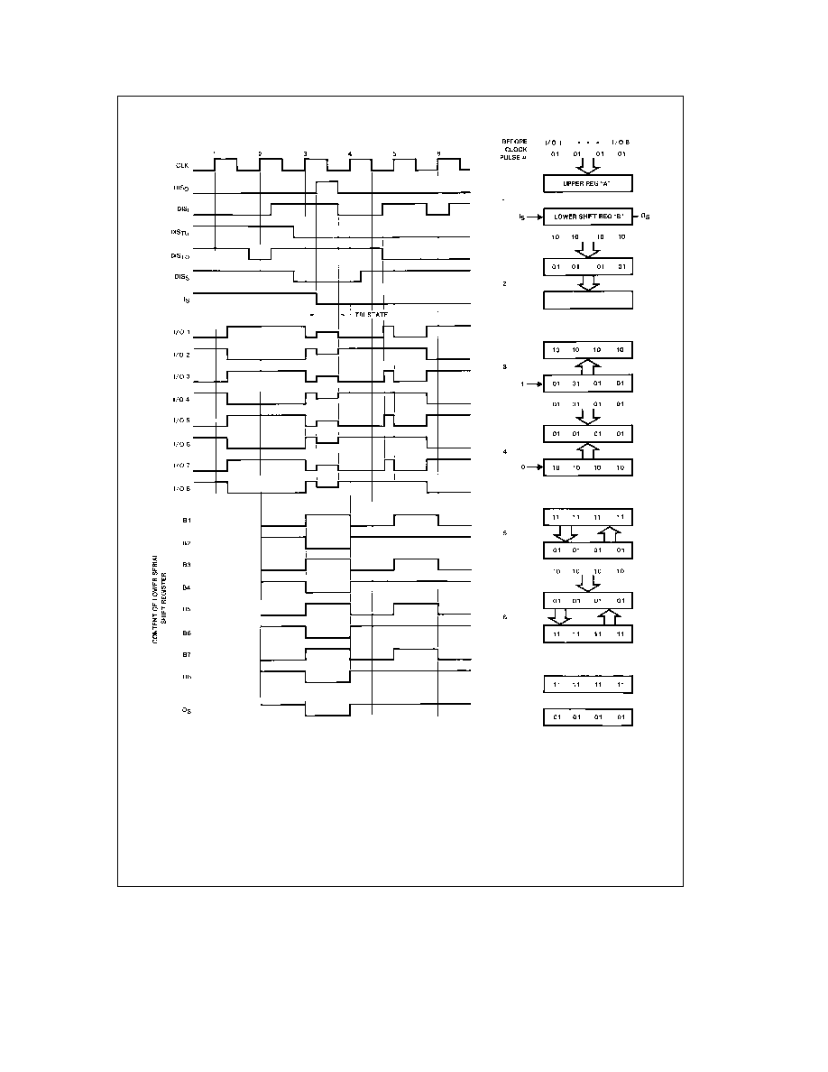
Timing Diagram
TL F 6438 ≠ 3
5