
TL D 9715
DM74S473
(512
x
8
)
4096-Bit
TTL
PROM
November 1990
DM74S473
(512 x 8) 4096-Bit TTL PROM
General Description
This Schottky memory is organized in the popular 512
words by 8 bits configuration A memory enable input is pro-
vided to control the output states When the device is en-
abled the outputs represent the contents of the selected
word When disabled the 8 outputs go to the ``OFF'' or high
impedance state
PROMs are shipped from the factory with lows in all loca-
tions A high may be programmed into any selected location
by following the programming instructions
Features
Y
Advanced titanium-tungsten (Ti-W) fuses
Y
Schottky-clamped for high speed
Address access
45 ns max
Enable access
30 ns max
Enable recovery
30 ns max
Y
PNP inputs for reduced input loading
Y
All DC and AC parameters guaranteed over
temperature
Y
Low voltage TRI-SAFE
TM
programming
Y
Open-collector outputs
Block Diagram
TL D 9715 � 1
Pin Names
A0 � A8
Addresses
G
Output Enable
GND
Ground
Q0 � Q7
Outputs
V
CC
Power Supply
TRI-SAFE
TM
is a trademark of National Semiconductor Corporation
C1995 National Semiconductor Corporation
RRD-B30M105 Printed in U S A

Connection Diagrams
Dual-In-Line Package
TL D 9715 � 2
Top View
Order Number DM74S473J 473AJ
DM74S473N or 473AN
See NS Package Number J20A or N20A
Plastic Leaded Chip Carrier (PLCC)
TL D 9715 � 3
Top View
Order Number DM74S473V or 473AV
See NS Package Number V20A
Ordering Information
Commercial Temp Range (0 C to
a
70 C)
Parameter Order Number
Max Access Time (ns)
DM74S473AN
45
DM74S473N
60
DM74S473AJ
45
DM74S473J
60
DM74S473AV
45
DM74S473V
60
2

Absolute Maximum Ratings
(Note 1)
If Military Aerospace specified devices are required
please contact the National Semiconductor Sales
Office Distributors for availability and specifications
Supply Voltage (Note 2)
b
0 5V to
a
7 0V
Input Voltage (Note 2)
b
1 2V to
a
5 5V
Output Voltage (Note 2)
b
0 5V to
a
5 5V
Storage Temperature
b
65 C to
a
150 C
Lead Temp (Soldering 10 seconds)
300 C
ESD to be determined
Note 1
Absolute maximum ratings are those values beyond which the de-
vice may be permanently damaged They do not mean that the device may
be operated at these values
Note 2
These limits do not apply during programming For the programming
ratings refer to the programming instructions
Operating Conditions
Min
Max
Units
Supply Voltage (V
CC
)
Commercial
4 75
5 25
V
Ambient Temperature (T
A
)
Commercial
0
a
70
C
Logical ``0'' Input Voltage
0
0 8
V
Logical ``1'' Input Voltage
2 0
5 5
V
DC Electrical Characteristics
(Note 1)
Symbol
Parameter
Conditions
DM74S473
Units
Min
Typ
Max
I
IL
Input Load Current
V
CC
e
Max V
IN
e
0 45V
b
80
b
250
m
A
I
IH
Input Leakage Current
V
CC
e
Max V
IN
e
2 7V
25
m
A
V
CC
e
Max V
IN
e
5 5V
1 0
mA
V
OL
Low Level Output Voltage
V
CC
e
Min I
OL
e
16 mA
0 35
0 45
V
V
IL
Low Level Input Voltage
0 80
V
V
IH
High Level Input Voltage
2 0
V
I
OZ
Output Leakage Current
V
CC
e
Max V
CEX
e
2 4V
50
m
A
(Open-Collector Only)
V
CC
e
Max V
CEX
e
5 5V
100
m
A
V
C
Input Clamp Voltage
V
CC
e
Min I
IN
e b
18 mA
b
0 8
b
1 2
V
C
I
Input Capacitance
V
CC
e
5 0V V
IN
e
2 0V
4 0
pF
T
A
e
25 C 1 MHz
C
O
Output Capacitance
V
CC
e
5 0V V
O
e
2 0V
6 0
pF
T
A
e
25 C 1 MHz Outputs Off
I
CC
Power Supply Current
V
CC
e
Max Input Grounded
110
155
mA
All Outputs Open
Note 1
These limits apply over the entire operating range unless stated otherwise All typical values are for V
CC
e
5 0V and T
A
e
25 C
3
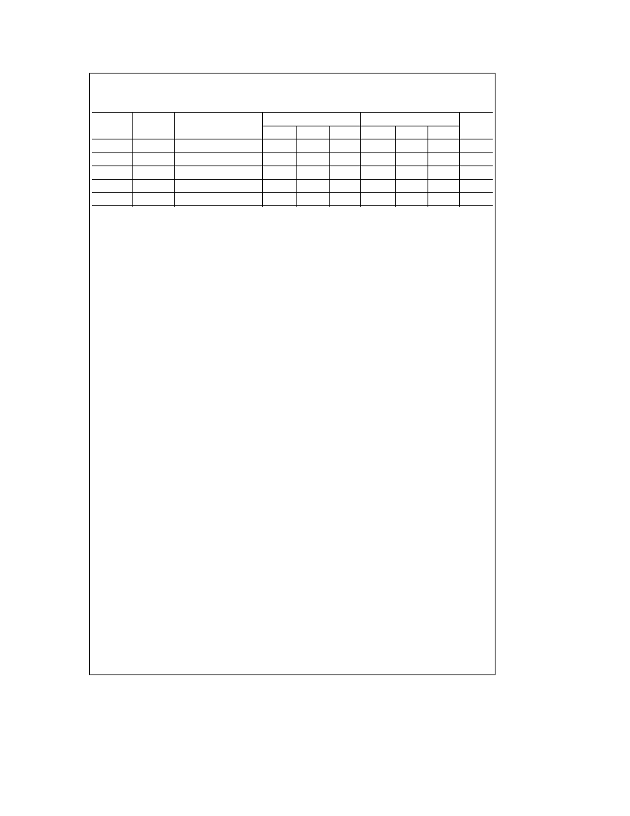
AC Electrical Characteristics
with Standard Load and Operating Conditions
COMMERCIAL TEMP RANGE
(0 C to
a
70 C)
Symbol
JEDEC
Parameter
DM74S473
DM74S473A
Units
Symbol
Min
Typ
Max
Min
Typ
Max
TAA
TAVQV
Address Access Time
40
60
25
45
ns
TEA
TEVQV
Enable Access Time
15
30
15
30
ns
TER
TEXQX
Enable Recovery Time
15
30
15
30
ns
TZX
TEVQX
Output Enable Time
15
30
15
30
ns
TXZ
TEXQZ
Output Disable Time
15
30
15
30
ns
Functional Description
TESTABILITY
The Schottky PROM die includes extra rows and columns of
fusable links for testing the programmability of each chip
These test fuses are placed at the worst-case chip locations
to provide the highest possible confidence in the program-
ming tests in the final product A ROM pattern is also per-
manently fixed in the additional circuitry and coded to pro-
vide a parity check of input address levels These and other
test circuits are used to test for correct operation of the row
and column-select circuits and functionality of input and en-
able gates All test circuits are available at both wafer and
assembled device levels to allow 100% functional and para-
metric testing at every stage of the test flow
RELIABILITY
As with all National products the Ti-W PROMs are subject-
ed to an on-going reliability evaluation by the Reliability As-
surance Department These evaluations employ accelerat-
ed life tests including dynamic high-temperature operating
life temperature-humidity life temperature cycling and ther-
mal shock To date nearly 7 4 million Schottky Ti-W PROM
device hours have been logged with samples in Epoxy B
molded DIP (N-package) PLCC (V-package) and CERIP (J-
package) Device performance in all package configurations
is excellent
TITANIUM-TUNGSTEN FUSES
National's Programmable Read-Only Memories (PROMs)
feature titanuim-tungsten (Ti-W) fuse links designed to pro-
gram efficiently with only 10 5V applied The high perform-
ance and reliability of these PROMs are the result of fabrica-
tion by a Schottky bipolar process of which the titanium-
tungsten metallization is an integral part and the use of an
on-chip programming circuit
A major advantage of the titanium-tungsten fuse technology
is the low programming voltage of the fuse links At 10 5V
this virtually eliminates the need for guard-ring devices and
wide spacings required for other fuse technologies Care is
taken however to minimize voltage drops across the die
and to reduce parasitics The device is designed to ensure
that worst-case fuse operating current is low enough for
reliable long-term operation The Darlington programming
circuit is liberally designed to insure adequate power density
for blowing the fuse links The complete circuit design is
optimized to provide high performance over the entire oper-
ating ranges of V
CC
and temperature
4

Physical Dimensions
inches (millimeters)
Ceramic Dual-In-Line Package (J)
Order Number DM74S473J or 473AJ
NS Package Number J20A
Molded Dual-In-Line Package (N)
Order Number DM74S473N or 473AN
NS Package Number N20A
5