TL F 6435
DM74LS465
(DM81LS95A)DM74LS466
(DM81LS96A)DM74LS467
(DM81LS97A)
DM74LS468
(DM81LS98A)
TRI-STATE
Octal
Buffer
September 1991
DM74LS465 (DM81LS95A) DM74LS466 (DM81LS96A)
DM74LS467 (DM81LS97A) DM74LS468 (DM81LS98A)
TRI-STATE
Octal Buffer
General Description
These devices provide eight two-input buffers in each pack-
age All employ the newest low-power-Schottky TTL tech-
nology One of the two inputs to each buffer is used as a
control line to gate the output into the high-impedance
state while the other input passes the data through the buff-
er The 'LS465 and 'LS467 present true data at the outputs
while the 'LS466 and 'LS468 are inverting On the 'LS465
and 'LS466 versions all eight TRI-STATE enable lines are
common with access through a 2-input NOR gate On the
'LS467 and 'LS468 versions four buffers are enabled from
one common line and the other four buffers are enabled
from another common line In all cases the outputs are
placed in the TRI-STATE condition by applying a high logic
level to the enable pins These devices represent octal low
power-Schottky versions of the very popular DM54 74365
366 367 and 368 (DM8095 96 97 and 98) TRI-STATE
hex buffers
Features
Y
Octal versions of popular DM74365 366 367 and 368
(DM8095 96 97 and 98)
Y
Typical power dissipation
LS465 467 (LS95A 97A)
80 mW
LS466 468 (LS96A 98A)
65 mW
Y
Typical propagation delay
LS465 467 (LS95A 97A)
15 ns
LS466 468 (LS96A 98A)
10 ns
Y
Low power-Schottky TRI-STATE technology
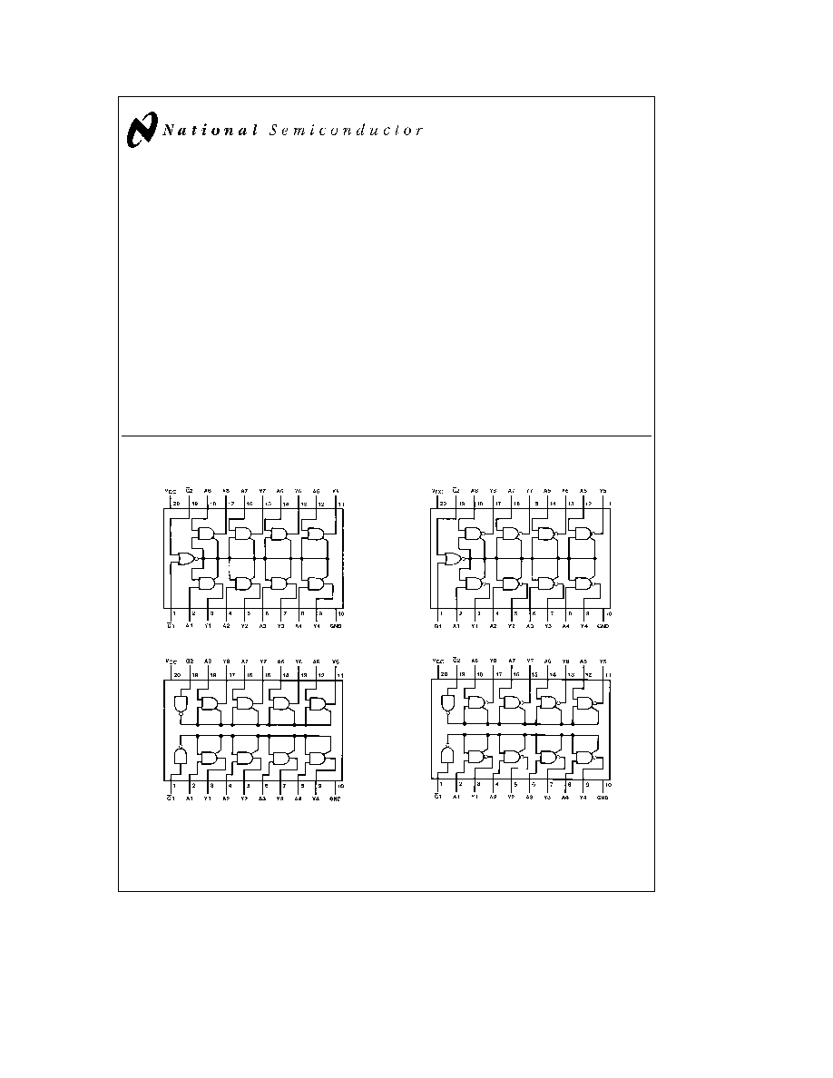
Connection Diagrams
Dual-In-Line Packages
TL F 6435 � 1
TL F 6435 � 3
TL F 6435 � 2
TL F 6435 � 4
Order Numbers DM74LS465WM DM81LS95AWM DM74LS465N DM81LS95AN
DM74LS466WM DM81LS96AWM DM74LS466N DM81LS96AN
DM74LS467WM DM81LS97AWM DM74LS467N DM81LS97AN
DM74LS468WM DM81LS98AWM or DM74LS468N DM81LS98AN
See NS Package Number M20B or N20A
TRI-STATE
is a registered trademark of National Semiconductor Corporation
C1995 National Semiconductor Corporation
RRD-B30M105 Printed in U S A
Absolute Maximum Ratings
(Note)
Supply Voltage
7V
Input Voltage
7V
Operating Free Air Temperature Range
DM74LS DM81LS
0 C to
a
70 C
Storage Temperature Range
b
65 C to
a
150 C
Note
The ``Absolute Maximum Ratings'' are those values
beyond which the safety of the device cannot be guaran-
teed The device should not be operated at these limits the
parametric values defined in the ``Electrical Characteristics''
table are not guaranteed at the absolute maximum ratings
The ``Recommended Operating Conditions'' table will define
the conditions for actual device operation
Recommended Operating Conditions
Symbol
Parameter
Min
Nom
Max
Units
V
CC
Supply Voltage
4 75
5
5 25
V
V
IH
High Level Input Voltage
2
V
V
IL
Low Level Input Voltage
0 8
V
I
OH
High Level Output Current
b
5 2
mA
I
OL
Low Level Output Current
24
mA
T
A
Free Air Operating Temperature
0
70
C
'LS465 ('LS95A) and 'LS467 ('LS97A) Electrical Characteristics
over recommended operating free air temperature range (unless otherwise noted)
Symbol
Parameter
Conditions
Min
Typ
Max
Units
(Note 1)
V
I
Input Clamp Voltage
V
CC
e
Min I
I
e b
18 mA
b
1 5
V
V
OH
High Level Output
V
CC
e
Min I
OH
e
Max
2 7
V
Voltage
V
IL
e
Max V
IH
e
Min
V
OL
Low Level Output
V
CC
e
Min I
OL
e
Max
0 5
Voltage
V
IL
e
Max V
IH
e
Min
V
I
OL
e
12 mA V
CC
e
Min
0 4
I
I
Input Current
Max
V
CC
e
Max V
I
e
7V
0 1
mA
Input Voltage
I
IH
High Level Input Current
V
CC
e
Max V
I
e
2 7V
20
m
A
I
IL
Low Level Input
V
CC
e
Max
V
I
e
0 5V
A (Note 3)
b
20
Current
V
I
e
0 4V
A (Note 4)
b
50
m
A
G
b
50
I
OZH
Off-State Output Current
V
CC
e
Max V
O
e
2 4V
with High Level Output
V
IH
e
Min V
IL
e
Max
20
m
A
Voltage Applied
I
OZL
Off-State Output Current
V
CC
e
Max V
O
e
0 4V
with Low Level Output
V
IH
e
Min V
IL
e
Max
b
20
m
A
Voltage Applied
I
OS
Short Circuit
V
CC
e
Max
b
20
b
100
mA
Output Current
(Note 2)
I
CC
Supply Current
V
CC
e
Max (Note 3)
16
26
mA
Note 1
All typicals are at V
CC
e
5V T
A
e
25 C
Note 2
Not more than one output should be shorted at a time and the duration should not exceed one second
Note 3
Both G inputs are at 2V
Note 4
Both G inputs are at 0 4V
2
'LS465 and 'LS467 Switching Characteristics
V
CC
e
5V T
A
e
25 C
R
L
e
667X
Symbol
Parameter
C
L
e
50 pF
C
L
e
150 pF
Units
Min
Max
Min
Max
t
PLH
Propagation Delay Time
16
25
ns
Low to High Level Output
t
PHL
Propagation Delay Time
28
40
ns
High to Low Level Output
t
PZH
Output Enable Time
25
30
ns
to High Level Output
t
PZL
Output Enable Time
30
42
ns
to Low Level Output
t
PHZ
Output Disable Time
20
ns
from High Level Output (Note 1)
t
PLZ
Output Disable Time
27
ns
from Low Level Output (Note 1)
Note 1
C
L
e
5 pF
'LS466 ('LS96A) and 'LS468 ('LS98A) Electrical Characteristics
over recommended operating free air temperature range (unless otherwise noted)
Symbol
Parameter
Conditions
Min
Typ
Max
Units
(Note 2)
V
I
Input Clamp Voltage
V
CC
e
Min I
I
e b
18 mA
b
1 5
V
V
OH
High Level Output
V
CC
e
Min I
OH
e
Max
2 7
V
Voltage
V
IL
e
Max V
IH
e
Min
V
OL
Low Level Output
V
CC
e
Min I
OL
e
Max
0 5
V
Voltage
V
IL
e
Max V
IH
e
Min
I
OL
e
12 mA V
CC
e
Min
0 4
I
I
Input Current
Max
V
CC
e
Max V
I
e
7V
0 1
mA
Input Voltage
I
IH
High Level Input Current
V
CC
e
Max V
I
e
2 7V
20
m
A
I
IL
Low Level Input
V
CC
e
Max
V
I
e
0 5V
A (Note 4)
b
20
Current
V
I
e
0 4V
A (Note 5)
b
50
m
A
G
b
50
I
OZH
Off-State Output Current
V
CC
e
Max V
O
e
2 4V
with High Level Output
V
IH
e
Min V
IL
e
Max
20
m
A
Voltage Applied
I
OZL
Off-State Output Current
V
CC
e
Max V
O
e
0 4V
with Low Level Output
V
IH
e
Min V
IL
e
Max
b
20
m
A
Voltage Applied
I
OS
Short Circuit
V
CC
e
Max
b
20
b
100
mA
Output Current
(Note 3)
I
CC
Supply Current
V
CC
e
Max (Note 5)
13
21
mA
Note 2
All typicals are at V
CC
e
5V T
A
e
25 C
Note 3
Not more than one output should be shorted at a time and the duration should not exceed one second
Note 4
Both G inputs are at 2V
Note 5
Both G inputs are at 0 4V
3

'LS466 and 'LS468 Switching Characteristics
for test waveforms and output load V
CC
e
5V T
A
e
25 C
R
L
e
667X
Symbol
Parameter
C
L
e
50 pF
C
L
e
150 pF
Units
Min
Max
Min
Max
t
PLH
Propagation Delay Time
10
16
ns
Low to High Level Output
t
PHL
Propagation Delay Time
17
30
ns
High to Low Level Output
t
PZH
Output Enable Time
15
30
ns
to High Level Output
t
PZL
Output Enable Time
35
45
ns
to Low Level Output
t
PHZ
Output Disable Time
20
ns
from High Level Output (Note 1)
t
PLZ
Output Disable Time
27
ns
from Low Level Output (Note 1)
Note 1
C
L
e
5 pF
Function Tables
LS465 (LS95A)
Inputs
Output
G1
G2
A
Y
H
X
X
Hi-Z
X
H
X
Hi-Z
L
L
H
H
L
L
L
L
LS467 (LS97A)
Inputs
Output
G
A
Y
H
X
Hi-Z
L
H
H
L
L
L
H
e
High Logic Level
L
e
Low Logic Level
X
e
Either High or Low Logic Level
Hi-Z
e
High Impedance (Off) State
LS466 (LS96A)
Inputs
Output
G1
G2
A
Y
H
X
X
Hi-Z
X
H
X
Hi-Z
L
L
H
L
L
L
L
H
LS468 (LS98A)
Inputs
Output
G
A
Y
H
X
Hi-Z
L
H
L
L
L
H
4
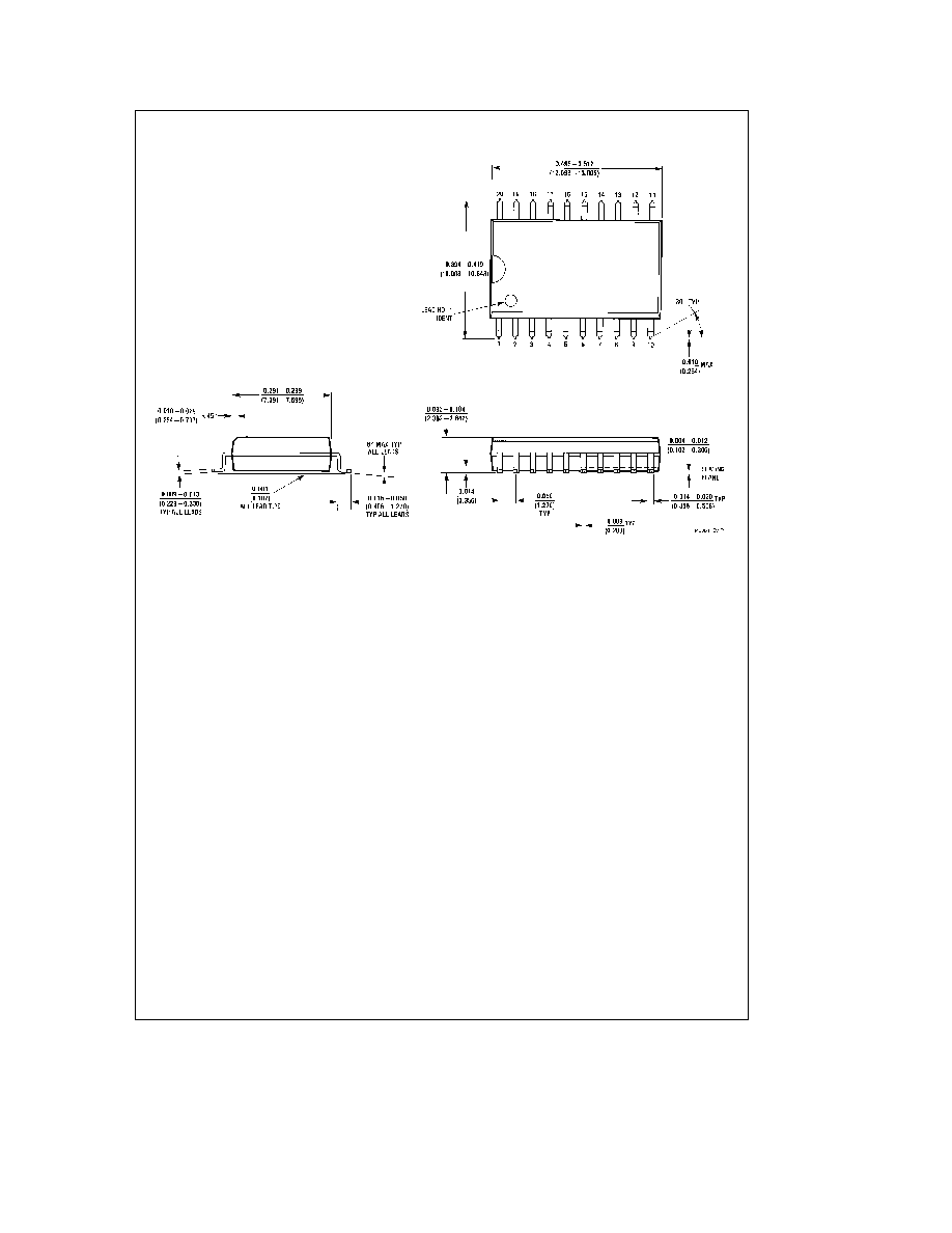
Physical Dimensions
inches (millimeters)
20-Lead Wide Small Outline Molded Package (M)
Order Numbers DM74LS465WM DM81LS95AWM DM74LS466WM DM81LS96AWM
DM74LS467WM DM81LS97AWM or DM74LS468WM DM81LS98AWM
NS Package Number M20B
5