TL F 6593
DM8898DM8899
TRI-STATE
BCD
to
BinaryBinary
to
BCD
Converters
January 1987
DM8898 DM8899 TRI-STATE
BCD to Binary Binary to BCD Converters
General Description
These circuits are the TRI-STATE versions of the popular
BCD to binary and binary to BCD converters DM74184 and
DM74185A respectively They are derived from the 256-bit
ROM DM8598 Emitter connections are made to provide
direct read out of converted codes at outputs Y8 through
Y1 as shown in the truth tables Both converters compre-
hend the fact that the least significant bits (LSB) of the bina-
ry and BCD codes are logically equal and in each case the
LSB bypasses the converter Thus a 6-bit converter is pro-
duced in each case and both devices are cascadable
An overriding enable input is provided on each converter
which when taken high inhibits the function causing all
outputs to go into the high-impedance state For this rea-
son and to minimize power consumption unused outputs
Y7 and Y8 of the 185A and all ``don't care'' conditions of the
184 are programmed high
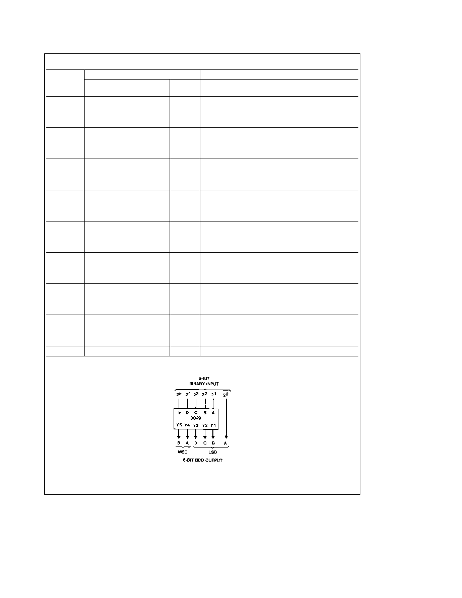
DM8898 BCD-TO-BINARY CONVERTERS
The 6-bit BCD-to-binary function of the DM8898 is analo-
gous to the algorithm
a Shift BCD number right one bit and examine each dec-
ade Subtract three from each 4-bit decade containing a
binary value greater than seven
b Shift right examine and correct after each shift until the
least significant decade contains a number smaller than
eight and all other converted decades contain zeros
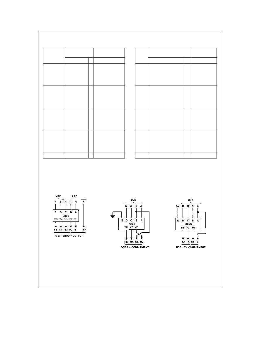
In addition to BCD-to-binary conversion the DM8898 is pro-
grammed to generate BCD 9's complement or BCD 10's
complement In each case one bit of the complement code
is logically equal to one of the BCD bits therefore these
complements can be produced on three lines As outputs
Y6 Y7 and Y8 are not required in the BCD-to-binary conver-
sion they are utilized to provide these complement codes
as specified in the function table when the devices are con-
nected as shown
DM8899A BINARY-TO-BCD CONVERTERS
The function performed by these 6-bit binary-to-BCD con-
verters is analogous to the algorithm
a Examine the three most significant bits If the sum is
greater than four add three and shift left one bit
b Examine each BCD decade If the sum is greater than
four add three and shift left one bit
c Repeat step b until the least-significant binary bit is in the
least-significant BCD location
Features
Y
TRI-STATE versions of DM74184 DM74185A
Y
Typical propagation delay 30 ns
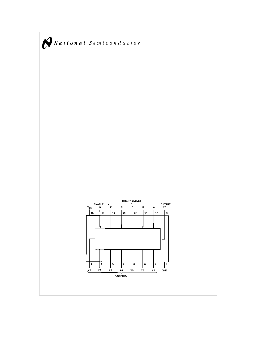
Connection Diagram
Dual-In-Line Package
TL F 6593 � 1
Order Number DM8898N or DM8899N
See NS Package Number N16A
TRI-STATE
is a registered trademark of National Semiconductor Corporation
C1995 National Semiconductor Corporation
RRD-B30M105 Printed in U S A
Absolute Maximum Ratings
(Note)
If Military Aerospace specified devices are required
please contact the National Semiconductor Sales
Office Distributors for availability and specifications
Supply Voltage
7V
Input Voltage
5 5V
Operating Free Air Temperature Range
DM88
0 C to
a
70 C
Storage Temperature Range
b
65 C to
a
150 C
Note
The ``Absolute Maximum Ratings'' are those values
beyond which the safety of the device cannot be guaran-
teed The device should not be operated at these limits The
parametric values defined in the ``Electrical Characteristics''
table are not guaranteed at the absolute maximum ratings
The ``Recommended Operating Conditions'' table will define
the conditions for actual device operation
Recommended Operating Conditions
Symbol
Parameter
DM8898
Units
Min
Nom
Max
V
CC
Supply Voltage
4 75
5
5 25
V
V
IH
High Level Input Voltage
2
V
V
IL
Low Level Input Voltage
0 8
V
I
OH
High Level Output Current
b
5 2
mA
I
OL
Low Level Output Current
12
mA
T
A
Free Air Operating Temperature
0
70
C
DM8898 Electrical Characteristics
over recommended operating free air temperature range (unless otherwise noted)
Symbol
Parameter
Conditions
Min
Typ
Max
Units
(Note 1)
V
I
Input Clamp Voltage
V
CC
e
Min I
I
e b
12 mA
b
1 5
V
V
OH
High Level Output
V
CC
e
Min I
OH
e
Max
2 4
V
Voltage
V
IL
e
Max V
IH
e
Min
V
OL
Low Level Output
V
CC
e
Min I
OL
e
Max
0 4
V
Voltage
V
IH
e
Min V
IL
e
Max
I
I
Input Current
Max
V
CC
e
Max V
I
e
5 5V
1
mA
Input Voltage
I
IH
High Level Input Current
V
CC
e
Max V
I
e
2 4V
40
m
A
I
IL
Low Level Input Current
V
CC
e
Max V
I
e
0 4V
b
1 6
mA
I
OZH
Off-State Output Current
V
CC
e
Max V
O
e
2 4V
with High Level
V
IH
e
Min V
IL
e
Max
40
m
A
Output Voltage Applied
I
OZL
Off-State Output Current
V
CC
e
Max V
O
e
0 4V
with Low Level
V
IH
e
Min V
IL
e
Max
b
40
m
A
Output Voltage Applied
I
OS
Short Circuit Output Current
V
CC
e
Max (Note 2)
b
20
b
70
mA
I
CC
Supply Current
V
CC
e
Max
70
99
mA
Note 1
All typicals are at V
CC
e
5V T
A
e
25 C
Note 2
Not more than one output should be shorted at a time
2
DM8898 Switching Characteristics
at V
CC
e
5V and T
A
e
25 C (See Section 1 for Test Waveforms and Output Load)
R
L
e
400X
Symbol
Parameter
C
L
e
5 pF
C
L
e
50 pF
Units
Min
Max
Min
Max
t
PLH
Propagation Delay Time
50
ns
Low to High Level Output
t
PHL
Propagation Delay Time
50
ns
High to Low Level Output
t
PZH
Output Enable Time
25
ns
to High Level Output
t
PZL
Output Enable Time
40
ns
to Low Level Output
t
PHZ
Output Disable Time
20
ns
from High Level Output
t
PLZ
Output Disable Time
36
ns
from Low Level Output
Recommended Operating Conditions
Symbol
Parameter
DM8899
Units
Min
Nom
Max
V
CC
Supply Voltage
4 75
5 0
5 25
V
V
IH
High Level Input Voltage
2
V
V
IL
Low Level Input Voltage
0 8
V
I
OH
High Level Output Current
b
5 2
mA
I
OL
Low Level Output Current
12
mA
T
A
Free Air Operating Temperature
0
70
C
3
DM8899 Electrical Characteristics
over recommended operating free air temperature range (unless otherwise noted)
Symbol
Parameter
Conditions
Min
Typ
Max
Units
(Note 1)
V
I
Input Clamp Voltage
V
CC
e
Min I
I
e b
12 mA
b
1 5
V
V
OH
High Level Output
V
CC
e
Min I
OH
e
Max
2 4
V
Voltage
V
IL
e
Max V
IH
e
Min
V
OL
Low Level Output
V
CC
e
Min I
OL
e
Max
0 4
V
Voltage
V
IH
e
Min V
IL
e
Max
I
I
Input Current
Max
V
CC
e
Max V
I
e
5 5V
1
mA
Input Voltage
I
IH
High Level Input Current
V
CC
e
Max V
I
e
2 4V
40
m
A
I
IL
Low Level Input Current
V
CC
e
Max V
I
e
0 4V
b
1 6
mA
I
OZH
Off-State Output Current
V
CC
e
Max V
O
e
2 4V
with High Level
V
IH
e
Min V
IL
e
Max
40
m
A
Output Voltage Applied
I
OZL
Off-State Output Current
V
CC
e
Max V
O
e
0 4V
with Low Level
V
IH
e
Min V
IL
e
Max
b
40
m
A
Output Voltage Applied
I
OS
Short Circuit Output Current
V
CC
e
Max (Note 2)
b
20
b
70
mA
I
CC
Supply Current
V
CC
e
Max
70
99
mA
DM8899 Switching Characteristics
at V
CC
e
5V and T
A
e
25 C (See Section 1 for Test Waveforms and Output Load)
R
L
e
400X
Symbol
Parameter
C
L
e
5 pF
C
L
e
50 pF
Units
Min
Max
Min
Max
t
PLH
Propagation Delay Time
50
ns
Low to High Level Output
t
PHL
Propagation Delay Time
50
ns
High to Low Level Output
t
PZH
Output Enable Time
25
ns
to High Level Output
t
PZL
Output Enable Time
40
ns
to Low Level Output
t
PHZ
Output Disable Time
20
ns
from High Level Output
t
PLZ
Output Disable Time
36
ns
from Low Level Output
Note 1
All typicals are at V
CC
e
5V T
A
e
25 C
Note 2
Not more than one output should be shorted at a time
4
Function Tables
BCD-to-Binary Converter
BCD
Inputs
Outputs
Words
(See Note A)
(See Note B)
E D C B A G Y5 Y4 Y3 Y2 Y1
0
1
L
L
L
L
L
L
L
L
L
L
L
2
3
L
L
L
L H L
L
L
L
L
H
4
5
L
L
L H L
L
L
L
L
H
L
6
7
L
L
L H H L
L
L
L
H
H
8
9
L
L H L
L
L
L
L
H
L
L
10
11
L H L
L
L
L
L
L
H
L
H
12
13
L H L
L H L
L
L
H
H
L
14
15
L H L H L
L
L
L
H
H
H
16
17
L H L H H L
L
H
L
L
L
18
19
L H H L
L
L
L
H
L
L
H
20
21
H L
L
L
L
L
L
H
L
H
L
22
23
H L
L
L H L
L
H
L
H
H
24
25
H L
L H L
L
L
H
H
L
L
26
27
H L
L H H L
L
H
H
L
H
28
29
H L H L
L
L
L
H
H
H
L
30
31
H H L
L
L
L
L
H
H
H
H
32
33
H H L
L H L
H
L
L
L
L
34
35
H H L H L
L
H
L
L
L
H
36
37
H H L H H L
H
L
L
H
L
38
39
H H H L
L
L
H
L
L
H
H
Any
X X X X X H
Z
Z
Z
Z
Z
BCD 9's or BCD 10's Complement Converter
BCD
Inputs
Outputs
Word
(See Note C)
(See Note D)
E
D
C
B
A
G
Y8
Y7
Y6
0
L
L
L
L
L
L
H
L
H
1
L
L
L
L
H
L
H
L
L
2
L
L
L
H
L
L
L
H
H
3
L
L
L
H
H
L
L
H
L
4
L
L
H
L
L
L
L
H
H
5
L
L
H
L
H
L
L
H
L
6
L
L
H
H
L
L
L
L
H
7
L
L
H
H
H
L
L
L
L
8
L
H
L
L
L
L
L
L
H
9
L
H
L
L
H
L
L
L
L
0
H
L
L
L
L
L
L
L
L
1
H
L
L
L
H
L
H
L
L
2
H
L
L
H
L
L
H
L
L
3
H
L
L
H
H
L
L
H
H
4
H
L
H
L
L
L
L
H
H
5
H
L
H
L
H
L
L
H
L
6
H
L
H
H
L
L
L
H
L
7
H
L
H
H
H
L
L
L
H
8
H
H
L
L
L
L
L
L
H
9
H
H
L
L
H
L
L
L
L
Any
X
X
X
X
X
H
Z
Z
Z
H
e
High Level L
e
Low Level Z
e
High Impedance
Note A
Input conditions other than those shown produce highs at outputs Y1 through Y5
Note B
Outputs Y6 Y7 and Y8 are not used for BCD-to-binary conversion
Note C
Input conditions other than those shown produce highs at outputs Y6 Y7 and Y8
Note D
Outputs Y1 through Y5 are not used for BCD 9's or BCD 10's complement conversion
When these devices are used as complement converters input E is used as a mode control With this input low the BCD 9's complement is generated when it is
high the BCD 10's complement is generated
6-Bit Converter
TL F 6593 � 2
BCD 9's
Complement Converter
TL F 6593 � 3
BCD 10's
Complement Converter
TL F 6593 � 4
5
Function Tables
(Continued)
Binary
Inputs
Outputs
Words
Binary Select
Enable
E
D
C
B
A
G
Y8
Y7
Y6
Y5
Y4
Y3
Y2
Y1
0
1
L
L
L
L
L
L
H
H
L
L
L
L
L
L
2
3
L
L
L
L
H
L
H
H
L
L
L
L
L
H
4
5
L
L
L
H
L
L
H
H
L
L
L
L
H
L
6
7
L
L
L
H
H
L
H
H
L
L
L
L
H
H
8
9
L
L
H
L
L
L
H
H
L
L
L
H
L
L
10
11
L
L
H
L
H
L
H
H
L
L
H
L
L
L
12
13
L
L
H
H
L
L
H
H
L
L
H
L
L
H
14
15
L
L
H
H
H
L
H
H
L
L
H
L
H
L
16
17
L
H
L
L
L
L
H
H
L
L
H
L
H
H
18
19
L
H
L
L
H
L
H
H
L
L
H
H
L
L
20
21
L
H
L
H
L
L
H
H
L
H
L
L
L
L
22
23
L
H
L
H
H
L
H
H
L
H
L
L
L
H
24
25
L
H
H
L
L
L
H
H
L
H
L
L
H
L
26
27
L
H
H
L
H
L
H
H
L
H
L
L
H
H
28
29
L
H
H
H
L
L
H
H
L
H
L
H
L
L
30
31
L
H
H
H
H
L
H
H
L
H
H
L
L
L
32
33
H
L
L
L
L
L
H
H
L
H
H
L
L
H
34
35
H
L
L
L
H
L
H
H
L
H
H
L
H
L
36
37
H
L
L
H
L
L
H
H
L
H
H
L
H
H
38
39
H
L
L
H
H
L
H
H
L
H
H
H
L
L
40
41
H
L
H
L
L
L
H
H
H
L
L
L
L
L
42
43
H
L
H
L
H
L
H
H
H
L
L
L
L
H
44
45
H
L
H
H
L
L
H
H
H
L
L
L
H
L
46
47
H
L
H
H
H
L
H
H
H
L
L
L
H
H
48
49
H
H
L
L
L
L
H
H
H
L
L
H
L
L
50
51
H
H
L
L
H
L
H
H
H
L
H
L
L
L
52
53
H
H
L
H
L
L
H
H
H
L
H
L
L
H
54
55
H
H
L
H
H
L
H
H
H
L
H
L
H
L
56
57
H
H
H
L
L
L
H
H
H
L
H
L
H
H
58
59
H
H
H
L
H
L
H
H
H
L
H
H
L
L
60
61
H
H
H
H
L
L
H
H
H
H
L
L
L
L
62
63
H
H
H
H
H
L
H
H
H
H
L
L
L
H
All
X
X
X
X
X
H
Z
Z
Z
Z
Z
Z
Z
Z
H
e
High Level L
e
Low Level X
e
Don't Care Z
e
High Impedance
6-Bit Converter
TL F 6593 � 5
6

7

DM8898DM8899
TRI-STATE
BCD
to
BinaryBinary
to
BCD
Converters
Physical Dimensions
inches (millimeters)
Molded Dual-In-Line Package (N)
Order Number DM8898N or DM8899AN
NS Package Number N16A
LIFE SUPPORT POLICY
NATIONAL'S PRODUCTS ARE NOT AUTHORIZED FOR USE AS CRITICAL COMPONENTS IN LIFE SUPPORT
DEVICES OR SYSTEMS WITHOUT THE EXPRESS WRITTEN APPROVAL OF THE PRESIDENT OF NATIONAL
SEMICONDUCTOR CORPORATION As used herein
1 Life support devices or systems are devices or
2 A critical component is any component of a life
systems which (a) are intended for surgical implant
support device or system whose failure to perform can
into the body or (b) support or sustain life and whose
be reasonably expected to cause the failure of the life
failure to perform when properly used in accordance
support device or system or to affect its safety or
with instructions for use provided in the labeling can
effectiveness
be reasonably expected to result in a significant injury
to the user
National Semiconductor
National Semiconductor
National Semiconductor
National Semiconductor
Corporation
Europe
Hong Kong Ltd
Japan Ltd
1111 West Bardin Road
Fax (a49) 0-180-530 85 86
13th Floor Straight Block
Tel 81-043-299-2309
Arlington TX 76017
Email cnjwge tevm2 nsc com
Ocean Centre 5 Canton Rd
Fax 81-043-299-2408
Tel 1(800) 272-9959
Deutsch Tel (a49) 0-180-530 85 85
Tsimshatsui Kowloon
Fax 1(800) 737-7018
English
Tel (a49) 0-180-532 78 32
Hong Kong
Fran ais Tel (a49) 0-180-532 93 58
Tel (852) 2737-1600
Italiano
Tel (a49) 0-180-534 16 80
Fax (852) 2736-9960
National does not assume any responsibility for use of any circuitry described no circuit patent licenses are implied and National reserves the right at any time without notice to change said circuitry and specifications