 | –≠–ª–µ–∫—Ç—Ä–æ–Ω–Ω—ã–π –∫–æ–º–ø–æ–Ω–µ–Ω—Ç: DM9314N | –°–∫–∞—á–∞—Ç—å:  PDF PDF  ZIP ZIP |

TL F 9788
9314DM9314
Quad
Latch
June 1989
9314 DM9314 Quad Latch
General Description
The '9314 is a multifunctional 4-bit latch designed for gener-
al purpose storage applications in high speed digital sys-
tems All outputs have active pull-up circuitry to provide high
capacitance drive and to provide low impedance in both
logic states for good noise immunity
Connection Diagram
Dual-In-Line Package
TL F 9788 ≠ 1
Order Number 9314DMQB 9314FMQB or DM9314N
See NS Package Number J16A N16E or W16A
Logic Symbol
TL F 9788 ≠ 2
V
CC
e
Pin 16
GND
e
Pin 8
Pin Names
Description
E
Enable Input (Active LOW)
D0 ≠ D3
Data Inputs
S0 ≠ S3
Set Inputs (Active LOW)
MR
Master Reset Input (Active LOW)
Q0 ≠ Q3
Latch Outputs
C1995 National Semiconductor Corporation
RRD-B30M115 Printed in U S A
Absolute Maximum Ratings
(Note)
If Military Aerospace specified devices are required
please contact the National Semiconductor Sales
Office Distributors for availability and specifications
Supply Voltage
7V
Input Voltage
5 5V
Operating Free Air Temperature Range
Military
b
55 C to
a
125 C
Commercial
0 C to
a
70 C
Storage Temperature Range
b
65 C to
a
150 C
Note
The ``Absolute Maximum Ratings'' are those values
beyond which the safety of the device cannot be guaran-
teed The device should not be operated at these limits The
parametric values defined in the ``Electrical Characteristics''
table are not guaranteed at the absolute maximum ratings
The ``Recommended Operating Conditions'' table will define
the conditions for actual device operation
Recommended Operating Conditions
Symbol
Parameter
Military
Commercial
Units
Min
Nom
Max
Min
Nom
Max
V
CC
Supply Voltage
4 5
5
5 5
4 75
5
5 25
V
V
IH
High Level Input Voltage
2
2
V
V
IL
Low Level Input Voltage
0 8
0 8
V
I
OH
High Level Output Current
b
0 8
b
0 8
mA
I
OL
Low Level Output Current
16
16
mA
T
A
Free Air Operating Temperature
b
55
125
0
70
C
t
s
(H)
Setup Time HIGH or LOW
5 0
5 0
ns
t
s
(L)
D
n
to E
18
18
t
h
(H)
Hold Time HIGH or LOW
0
0
ns
t
h
(L)
D
n
to E
5 0
5 0
t
s
(H)
Setup Time HIGH D
n
to S
n
8 0
8 0
ns
t
h
(L)
Hold Time LOW D
n
to S
n
8 0
8 0
ns
t
w
(L)
E Pulse Width LOW
18
18
ns
t
w
(L)
MR Pulse Width LOW
18
18
ns
t
rec
Recovery Time MR to E
0
0
ns
Electrical Characteristics
Over recommended operating free air temperature range (unless otherwise noted)
Symbol
Parameter
Conditions
Min
Typ
Max
Units
(Note 1)
V
I
Input Clamp Voltage
V
CC
e
Min I
I
e b
12 mA
b
1 5
V
V
OH
High Level Output Voltage
V
CC
e
Min I
OH
e
Max
2 4
3 4
V
V
IL
e
Max
V
OL
Low Level Output Voltage
V
CC
e
Min I
OL
e
Max
0 2
0 4
V
V
IH
e
Min
I
I
Input Current
Max
V
CC
e
Min V
I
e
5 5V
1
mA
Input Voltage
I
IH
High Level Input Current
V
CC
e
Max V
I
e
2 4V
40
m
A
Data Inputs
60
I
IL
Low Level Input Current
V
CC
e
Max V
I
e
0 4V
b
1 6
mA
Data Inputs
b
2 7
I
OS
Short Circuit
V
CC
e
Max
MIL
b
20
b
70
mA
Output Current
(Note 2)
COM
b
20
b
70
I
CC
Supply Current
V
CC
e
Max
55
mA
Note 1
All typicals are at V
CC
e
5V T
A
e
25 C
Note 2
Not more than one output should be shorted at a time
2

Switching Characteristics
V
CC
e a
5 0V T
A
e a
25 C (See Section 1 for waveforms and load configurations)
Symbol
Parameter
C
L
e
15 pF
Units
Min
Max
t
PLH
Propagation Delay
24
ns
t
PHL
E to Q
n
24
t
PLH
Propagation Delay
12
ns
t
PHL
D
n
to Q
n
24
t
PLH
Propagation Delay
18
ns
MR to Q
n
t
PHL
Propagation Delay
24
ns
S
n
to Q
n
Functional Description
The '9314 consists of four latches with a common active
LOW Enable input and active LOW Master Reset input
When the Enable goes HIGH data present in the latches is
stored and the state of the latch is no longer affected by the
S
n
and D
n
inputs The Master Reset when activated over-
rides all other input conditions forcing all latch outputs LOW
Each of the four latches can be operated in one of two
modes
D-TYPE LATCH
For D-type operation the S input of a latch
is held LOW While the common Enable is active the latch
output follows the D input Information present at the latch
output is stored in the latch when the Enable goes HIGH
SET RESET LATCH
During set reset operation when the
common Enable is LOW a latch is reset by a LOW on the D
input and can be set by a LOW on the S input if the D input
is HIGH If both S and D inputs are LOW the D input will
dominate and the latch will be reset When the Enable goes
HIGH the latch remains in the last state prior to disable-
ment The two modes of latch operation are shown in the
Truth Table
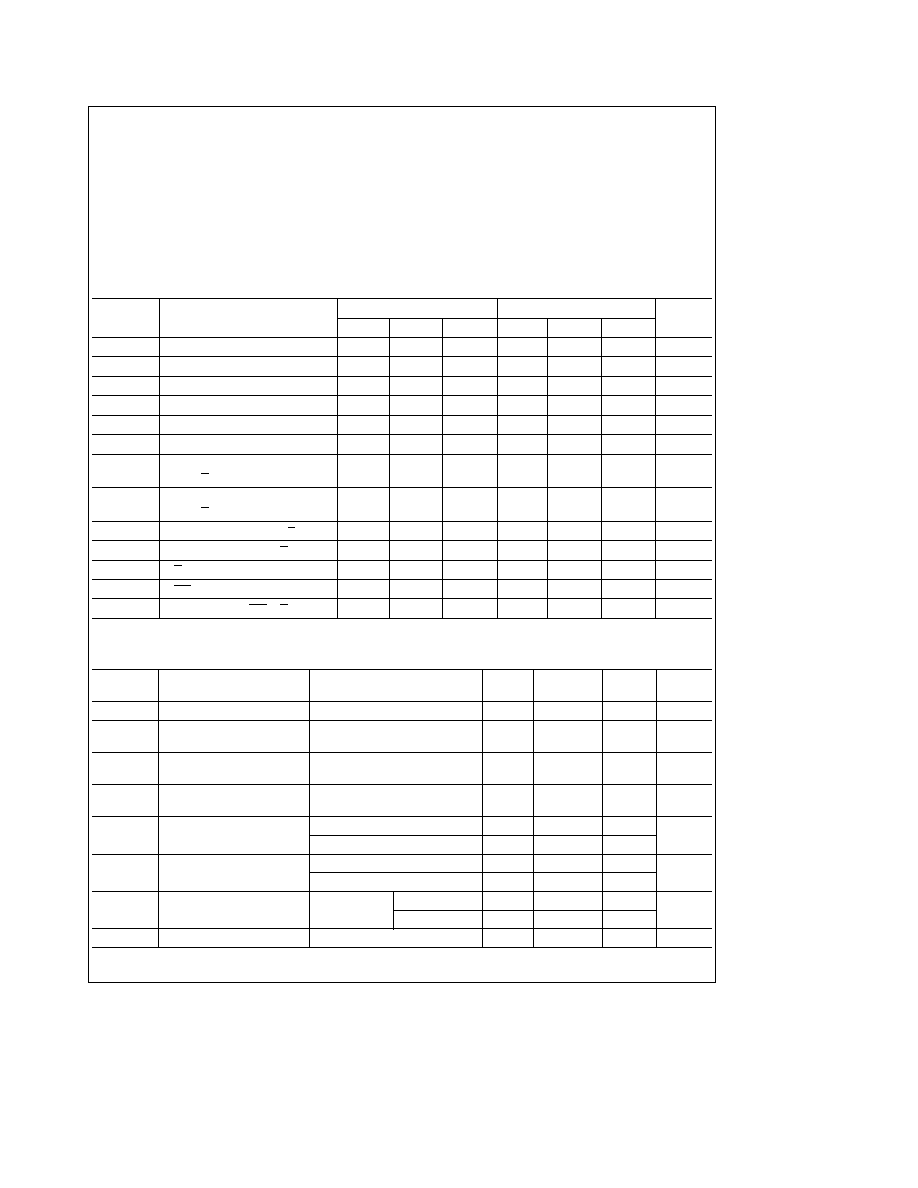
Truth Table
MR
E
D
S
Q
n
Operation
H
L
L
L
L
D Mode
H
L
H
L
H
H
H
X
X
Q
nb1
H
L
L
L
L
R S Mode
H
L
H
L
H
H
L
L
H
L
H
L
H
H
Q
nb1
H
H
X
X
Q
nb1
L
X
X
X
L
Reset
H
e
HIGH Voltage Level
L
e
LOW Voltage Level
X
e
Immaterial
Q
n
b
1
e
Previous Output State
Q
n
e
Present Output State
3
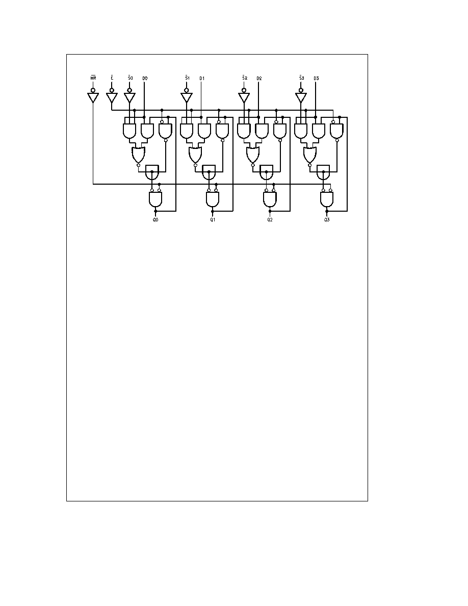
Logic Diagram
TL F 9788 ≠ 3
4

Physical Dimensions
inches (millimeters)
16-Lead Ceramic Dual-In-Line Package (J)
Order Number 9314DMQB
NS Package Number J16A
16-Lead Molded Dual-In-Line Package (N)
Order Number DM9314N
NS Package Number N16E
5

9314DM9314
Quad
Latch
Physical Dimensions
inches (millimeters) (Continued)
16-Lead Ceramic Flat Package (W)
Order Number 9314FMQB
NS Package Number W16A
LIFE SUPPORT POLICY
NATIONAL'S PRODUCTS ARE NOT AUTHORIZED FOR USE AS CRITICAL COMPONENTS IN LIFE SUPPORT
DEVICES OR SYSTEMS WITHOUT THE EXPRESS WRITTEN APPROVAL OF THE PRESIDENT OF NATIONAL
SEMICONDUCTOR CORPORATION As used herein
1 Life support devices or systems are devices or
2 A critical component is any component of a life
systems which (a) are intended for surgical implant
support device or system whose failure to perform can
into the body or (b) support or sustain life and whose
be reasonably expected to cause the failure of the life
failure to perform when properly used in accordance
support device or system or to affect its safety or
with instructions for use provided in the labeling can
effectiveness
be reasonably expected to result in a significant injury
to the user
National Semiconductor
National Semiconductor
National Semiconductor
National Semiconductor
Corporation
Europe
Hong Kong Ltd
Japan Ltd
1111 West Bardin Road
Fax (a49) 0-180-530 85 86
13th Floor Straight Block
Tel 81-043-299-2309
Arlington TX 76017
Email cnjwge tevm2 nsc com
Ocean Centre 5 Canton Rd
Fax 81-043-299-2408
Tel 1(800) 272-9959
Deutsch Tel (a49) 0-180-530 85 85
Tsimshatsui Kowloon
Fax 1(800) 737-7018
English
Tel (a49) 0-180-532 78 32
Hong Kong
Fran ais Tel (a49) 0-180-532 93 58
Tel (852) 2737-1600
Italiano
Tel (a49) 0-180-534 16 80
Fax (852) 2736-9960
National does not assume any responsibility for use of any circuitry described no circuit patent licenses are implied and National reserves the right at any time without notice to change said circuitry and specifications