 | –≠–ª–µ–∫—Ç—Ä–æ–Ω–Ω—ã–π –∫–æ–º–ø–æ–Ω–µ–Ω—Ç: DM9321N | –°–∫–∞—á–∞—Ç—å:  PDF PDF  ZIP ZIP |
TL F 10209
9321DM9321
Dual
1-of-4
Decoder
June 1989
9321 DM9321
Dual 1-of-4 Decoder
General Description
The 9321 consists of two independent multipurpose decod-
ers each designed to accept two inputs and provide four
mutually exclusive outputs In addition an active LOW en-
able input which gives demultiplexing capability is provided
for each decoder
Features
Y
Multifunction capability
Y
Mutually exclusive outputs
Y
Demultiplexing capability
Y
Active low enable for each decoder
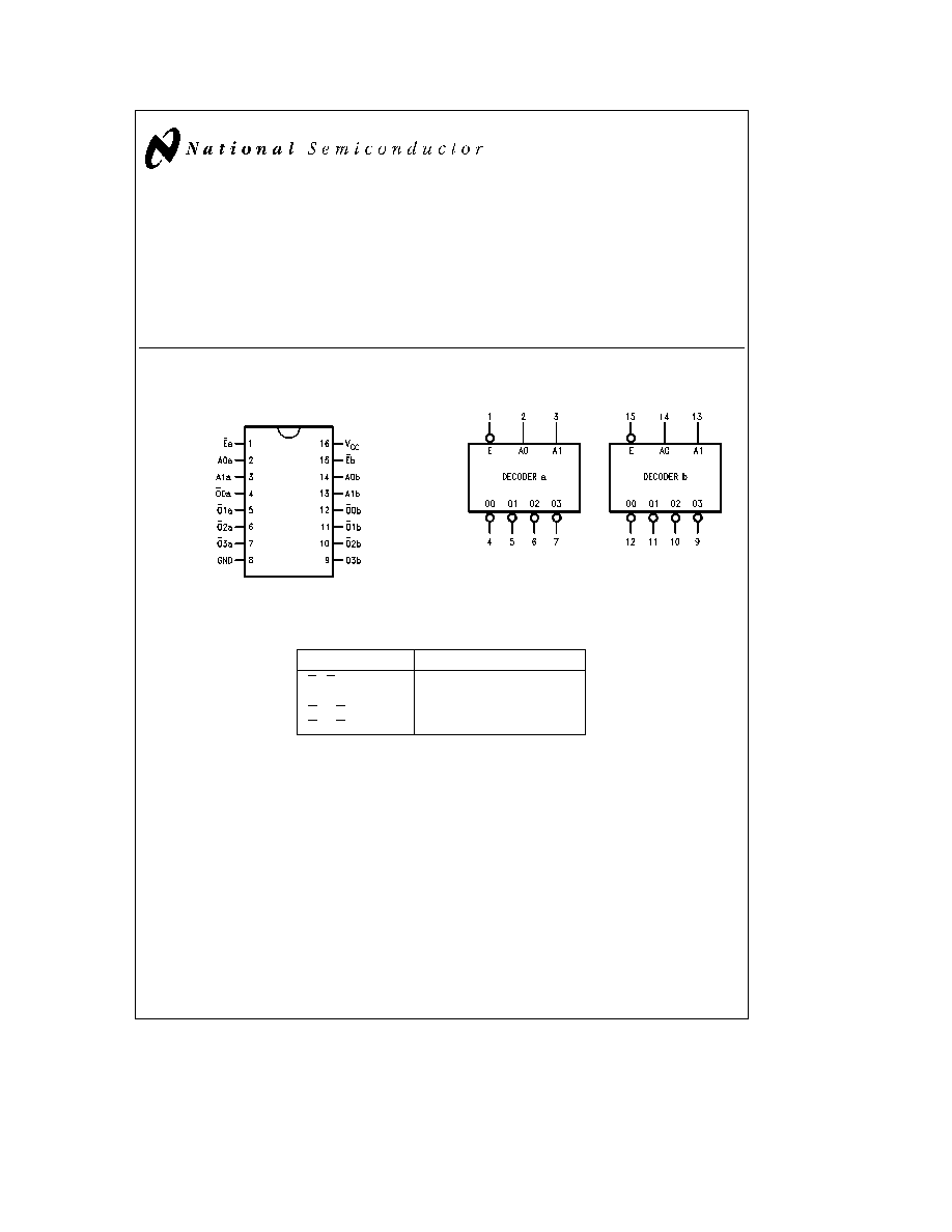
Connection Diagram
Dual-In-Line Package
TL F 10209 ≠ 1
Order Number 9321DMQB 9321FMQB or DM9321N
See NS Package Number J16A N16E or W16A
Logic Symbol
TL F 10209 ≠ 2
V
CC
e
Pin 16
GND
e
Pin 8
Pin Names
Description
Ea Eb
Enable Inputs (Active LOW)
A0a A1a A0b A1b
Address Inputs
O0a ≠ O3a
Decoder Outputs (Active LOW)
O0b ≠ O3b
(
C1995 National Semiconductor Corporation
RRD-B30M105 Printed in U S A
Absolute Maximum Ratings
(Note)
If Military Aerospace specified devices are required
please contact the National Semiconductor Sales
Office Distributors for availability and specifications
Supply Voltage
7V
Input Voltage
5 5V
Operating Free Air Temperature Range
MIL
b
55 C to
a
125 C
COMM
0 C to
a
70 C
Storage Temperature Range
b
65 C to
a
150 C
Note
The ``Absolute Maximum Ratings'' are those values
beyond which the safety of the device cannot be guaran-
teed The device should not be operated at these limits The
parametric values defined in the ``Electrical Characteristics''
table are not guaranteed at the absolute maximum ratings
The ``Recommended Operating Conditions'' table will define
the conditions for actual device operation
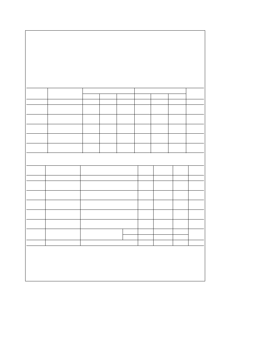
Recommended Operating Conditions
Symbol
Parameter
Military
Commercial
Units
Min
Nom
Max
Min
Nom
Max
V
CC
Supply Voltage
4 5
5
5 5
4 75
5
5 25
V
V
IH
High Level Input
2
2
V
Voltage
V
IL
Low Level Input
0 8
0 8
V
Voltage
I
OH
High Level Output
b
0 8
b
0 8
mA
Current
I
OL
Low Level Output
16
16
mA
Current
T
A
Free Air Operating
b
55
125
0
70
C
Temperature
Electrical Characteristics
over recommended operating free air temperature (unless otherwise noted)
Symbol
Parameter
Conditions
Min
Typ
Max
Units
(Note 1)
V
I
Input Clamp Voltage
V
CC
e
Min I
I
e b
10 mA
b
1 5
V
V
OH
High Level Output
V
CC
e
Min I
OH
e
Max
2 4
V
Voltage
V
IL
e
Max V
IH
e
Min
V
OL
Low Level Output
V
CC
e
Min I
OL
e
Max
0 4
V
Voltage
V
IH
e
Min V
IL
e
Max
I
I
Input Current
Max
V
CC
e
Max V
I
e
5 5V
1
mA
Input Voltage
I
IH
High Level Input
V
CC
e
Max V
I
e
2 4V
40
m
A
Current
I
IL
Low Level Input
V
CC
e
Max V
I
e
0 4V
b
1 6
mA
Current
I
OS
Short Circuit
V
CC
e
Max
MIL
b
20
b
70
mA
Output Current
(Note 2)
COM
b
1 3
b
3 7
I
CC
Supply Current
V
CC
e
Max (Note 3)
50
mA
Note 1
All typicals are at V
CC
e
5V T
A
e
25 C
Note 2
Not more than one output should be shorted at a time and the duration should not exceed one second
Note 3
I
CC
is measured with all outputs open and all inputs grounded
2
Switching Characteristics
V
CC
e a
5 0V T
A
e a
25 C (See Section 1 for test waveforms and output load)
Symbol
Parameter
C
L
e
15 pF
Units
Min
Max
t
PLH
Propagation Delay An to On
20
ns
t
PHL
21
t
PLH
Propagation Delay E to On
14
ns
t
PHL
18
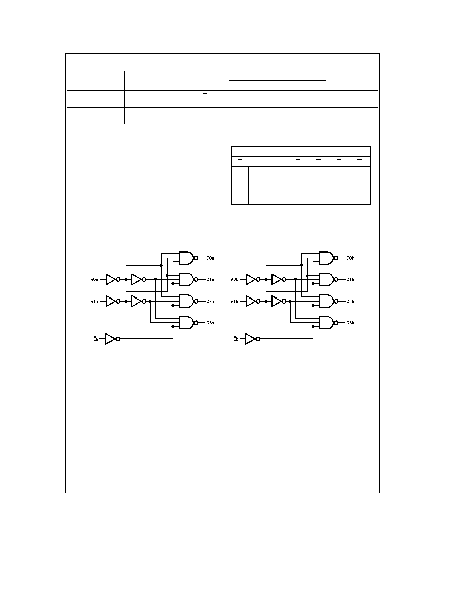
Functional Description
The 9321 consists of two separate decoders each designed
to accept two binary weighted inputs and provide four mutu-
ally exclusive active LOW outputs as shown in the logic
symbol Each decoder can be used as a 4-output demulti-
plexer by using the enable as a data input
Truth Table
(Each Decoder)
Inputs
Outputs
E
A0
A1
O0
O1
O2
O3
L
L
L
L
H
H
H
L
H
L
H
L
H
H
L
L
H
H
H
L
H
L
H
H
H
H
H
L
H
X
X
H
H
H
H
H
e
HIGH Voltage Level
L
e
LOW Voltage Level
X
e
Immaterial
Logic Diagram
TL F 10209 ≠ 3
3

4
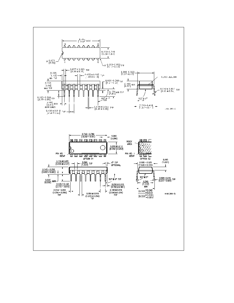
Physical Dimensions
inches (millimeters)
16-Lead Ceramic Dual-In-Line Package (J)
Order Number 9321DMQB
NS Package Number J16A
16 Lead Molded Dual-In-Line Package (N)
Order Number DM9321N
NS Package Number N16E
5