TL F 6824
DP8212DP8212M
8-Bit
InputOutput
Port
June 1988
DP8212 DP8212M 8-Bit Input Output Port
General Description
The DP8212 DP8212M is an 8-bit input output port con-
tained in a standard 24-pin dual-in-line package The device
which is fabricated using Schottky Bipolar technology is
part of National Semiconductor's 8080A support family The
DP8212 DP8212M can be used to implement latches gat-
ed buffers or multiplexers Thus all of the major peripheral
and input output functions of a microcomputer system can
be implemented with this device
The
DP8212 DP8212M
includes
an
8-bit
latch
with
TRI-STATE
output buffers and device selection and con-
trol logic Also included is a service request flip-flop for the
generation and control of interrupts to the microprocessor
Features
Y
8-Bit data latch and buffer
Y
Service request flip-flop for generation and control of
interrupts
Y
0 25 mA input load current
Y
TRI-STATE TTL output drive capability
Y
Outputs sink 15 mA
Y
Asynchronous latch clear
Y
3 65V output for direct interface to INS8080A
Y
Reduces system package count by replacing buffers
latches and multiplexers in microcomputer systems
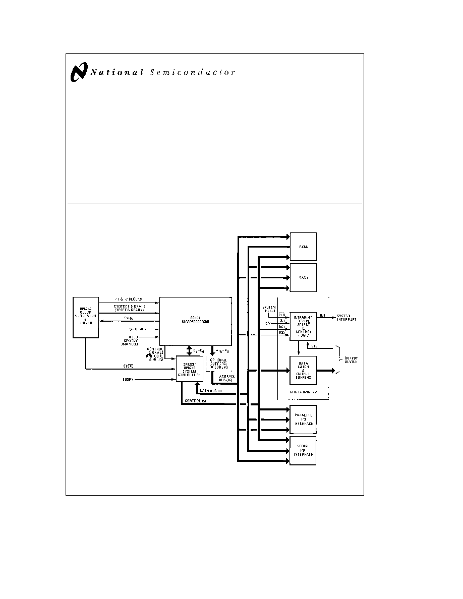
8080A Microcomputer Family Block Diagram
TL F 6824 � 1
TRI-STATE
is a registered trademark of National Semiconductor Corp
C1995 National Semiconductor Corporation
RRD-B30M105 Printed in U S A
Absolute Maximum Ratings
If Military Aerospace specified devices are required
please contact the National Semiconductor Sales
Office Distributors for availability and specifications
Storage Temperature
b
65 C to
a
160 C
All Output or Supply Voltages
b
0 5V to
a
7V
All Input Voltages
b
1 0V to 5 5V
Output Currents
125 mA
Maximum Power Dissipation at 25 C
Cavity Package
1903 mW
Molded Package
2005 mW
Derate cavity package 12 7 mW C above 25 C derate molded package
16 0 mW C above 25 C
Operating Conditions
Min
Max
Units
Supply Voltage (V
CC
)
DP8212M
4 50
5 50
V
DC
DP8212
4 75
5 25
V
DC
Operating Temperaure (T
A
)
DP8212M
b
55
a
125
C
DP8212
0
a
75
C
Note
Maximum ratings indicate limits beyond which perma-
nent damage may occur Continuous operation at these lim-
its is not intended and should be limited to those conditions
specified under DC electrical characteristics
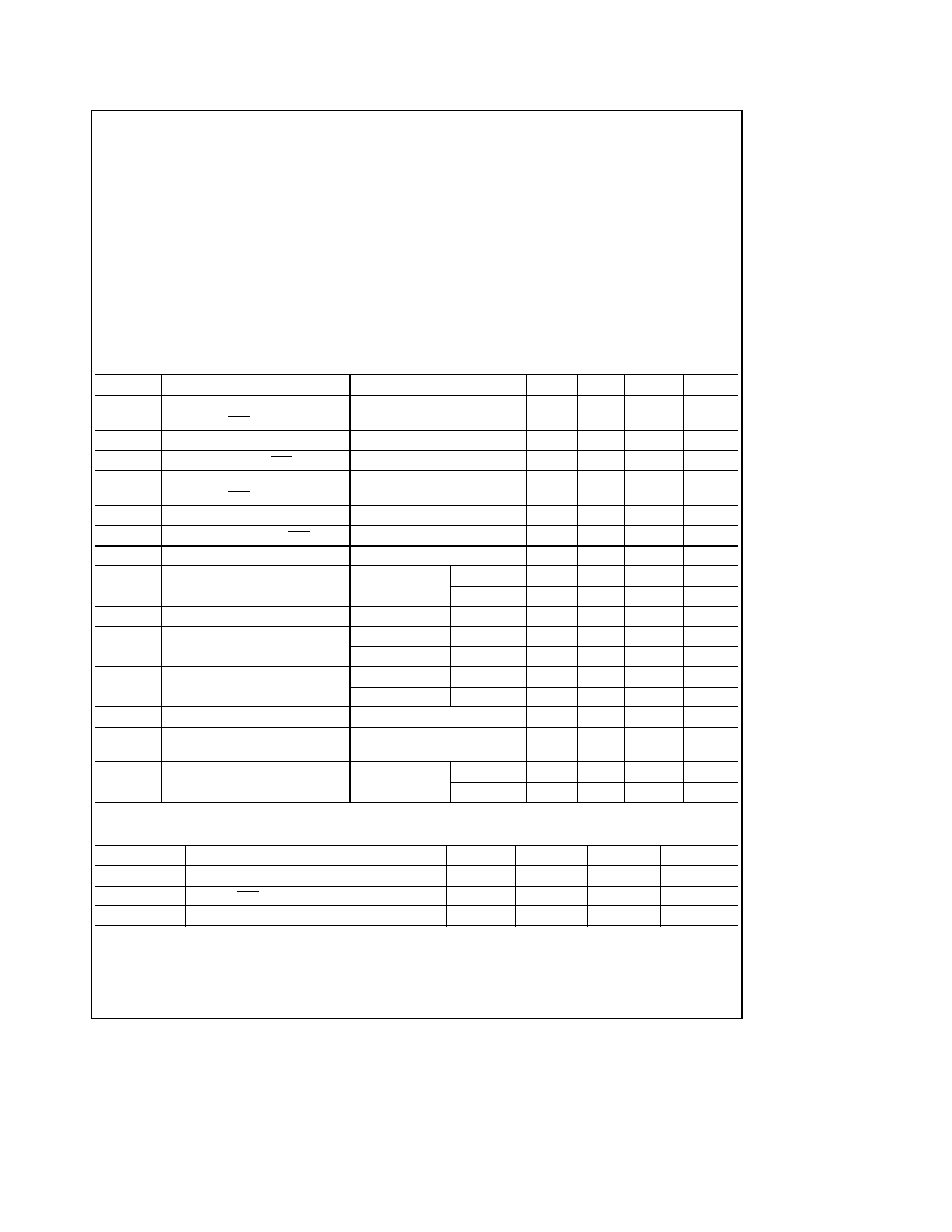
Electrical Characteristics
Min
s
T
A
s
Max Min
s
V
CC
s
Max unless otherwise noted
Symbol
Parameter
Conditions
Min
Typ
Max
Units
I
F
Input Load Current
V
F
e
0 45V
b
0 25
mA
STB DS2 CLR DI
1
� DI
8
Inputs
I
F
Input Load Current MD Input
V
F
e
0 45V
b
0 75
mA
I
F
Input Load Current DS1 Input
V
F
e
0 45V
b
1 0
mA
I
R
Input Leakage Current
V
R
e
V
CC
Max
10
m
A
STB DS2 CLR DI
1
� DI
8
Inputs
I
R
Input Leakage Current MD Input
V
R
e
V
CC
Max
30
m
A
I
R
Input Leakage Current DS1 Input
V
R
e
V
CC
Max
40
m
A
V
C
Input Forward Voltage Clamp
I
C
e b
5 mA
b
1
V
V
IL
Input ``Low'' Voltage
DP8212M
0 08
V
DP8212
0 85
V
V
IH
Input ``High'' Voltage
2 0
V
V
OL
Output ``Low'' Voltage
I
OL
e
10 mA
DP8212M
0 45
V
I
OL
e
15 mA
DP8212
0 45
V
V
OH
Output ``High'' Voltage
I
OH
e
0 5 mA
DP8212M
3 40
4 0
V
I
OH
e
1 0 mA
DP8212
3 65
4 0
V
I
SC
Short-Circuit Output Current
V
O
e
0V V
CC
e
5V
b
15
b
75
mA
l
I
O
l
Output Leakage Current High
V
O
e
0 45V V
CC
Max
20
m
A
Impedance State
I
CC
Power Supply Current
DP8212M
90
145
mA
DP8212
90
130
mA
Capacitance
F
e
1 MHz V
BIAS
e
2 5V V
CC
e
5V T
A
e
25 C
Symbol
Parameter
Min
Typ
Max
Units
C
IN
DS1 MD Input Capacitance
9
12
pF
C
IN
DS2 CLR STB DI
1
� DI
8
Input Capacitance
5
9
pF
C
OUT
DO1 � DO8 Output Capacitance
8
12
pF
This parameter is sampled and not 100% tested
2
Switching Characteristics
Min
s
T
A
s
Max Min
s
V
CC
s
Max
Symbol
Parameter
Conditions
DP8212M
DP8212
Units
Min
Max
Min
Max
t
PW
Pulse Width
40
30
ns
t
PD
Data to Output Delay
(Note 1)
30
30
ns
t
WE
Write Enable to Output Delay
(Note 1)
50
40
ns
t
SET
Data Set-Up Time
20
15
ns
t
H
Data Hold Time
30
20
ns
t
R
Reset to Output Delay
(Note 1)
55
40
ns
t
S
Set to Output Delay
(Note 1)
35
30
ns
t
E
Output Enable Disable Time
(Note 2)
50
45
ns
t
C
Clear to Output Delay
(Note 1)
65
55
ns
Note 1
C
L
e
30 pF
Note 2
C
L
e
30 pF except for DP8212M
t
E (DISABLE)
C
L
e
5 pF
Switching Conditions
1 Input Pulse Amplitude
e
2 5V
2 Input Rise and Fall Times
e
5 ns
3 Between 1V and 2V Measurements made at 1 5V with 15 mA
30 pF Test Load
4 C
L
includes jig and probe capacitance
5 C
L
e
30 pF
6 C
L
e
30 pF except for DP8212M t
E (DISABLE)
C
L
e
5 pF
Test Load
TL F 6824 � 2
Alternate Test Load
(Refer to Timing Diagram)
TL F 6824 � 3
3
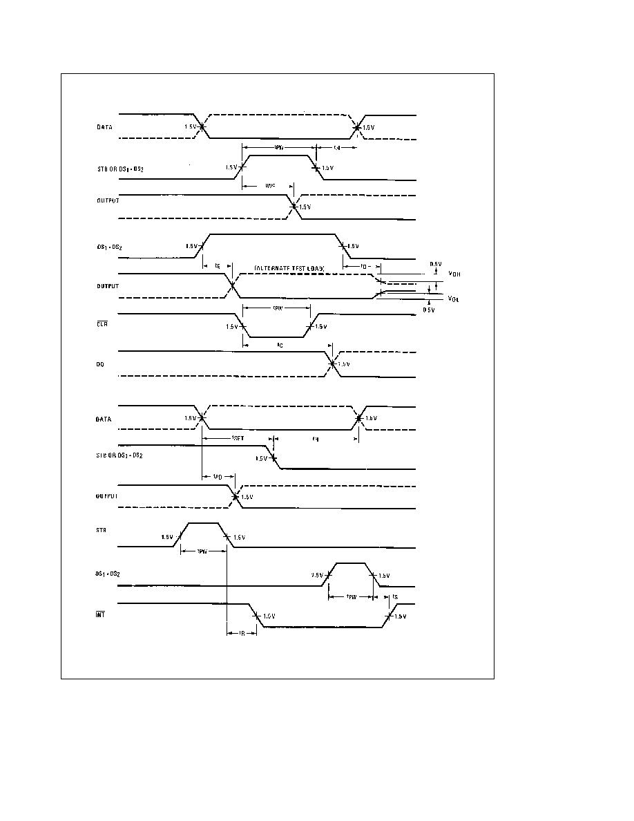
Timing Diagram
TL F 6824 � 4
4
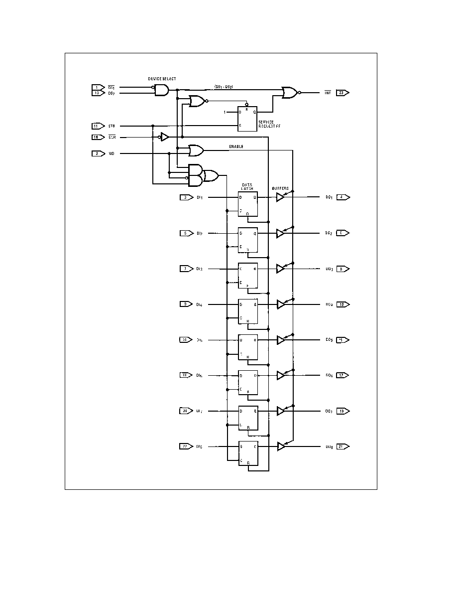
Logic Diagram
TL F 6824 � 5
5
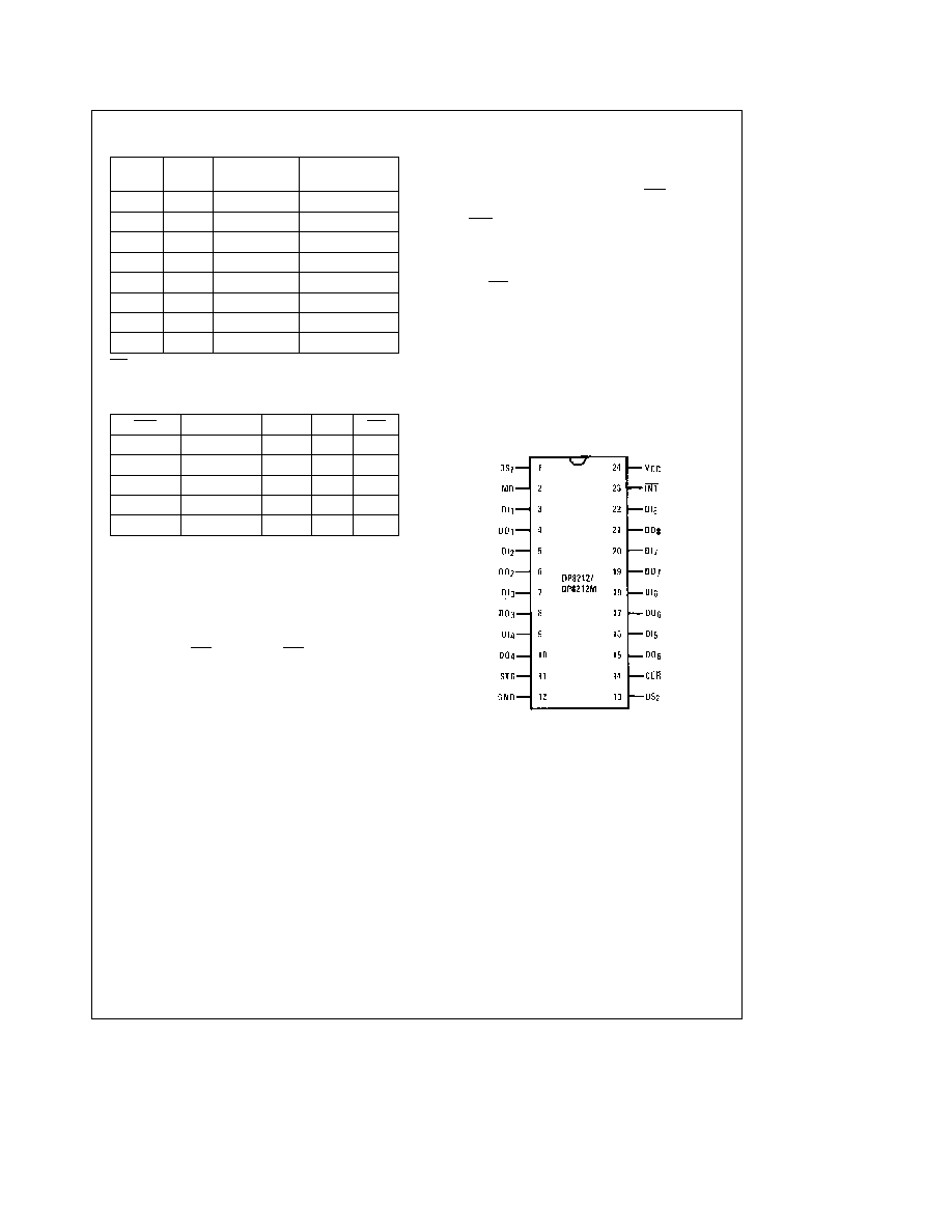
Logic Tables
Logic Table A
STB
MD
(DS
1
DS
2
)
Data Out
Equals
0
0
0
TRI-STATE
1
0
0
TRI-STATE
0
1
0
DATA LATCH
1
1
0
DATA LATCH
0
0
1
DATA LATCH
1
0
1
DATA IN
0
1
1
DATA IN
1
1
1
DATA IN
CLR
K resets data latch to the output low state
The data latch clock is level sensitive a low level clock latches the data
Logic Table B
CLR
(DS
1
DS
2
)
STB
Q
INT
0 RESET
0
0
0
1
1
0
0
0
1
1
0
K
1
0
1
1 RESET
0
0
0
1
0
0
0
1
Internal Service Request flip-flop
Functional Pin Definitions
The following describes the function of all the DP8212
DP8212M input output pins Some of these descriptions
reference internal circuits
INPUT SIGNALS
Device Select (DS
1
DS
2
)
When DS
1
is low and DS
2
is
high the device is selected The output buffers are enabled
and the service request flip-flop is asynchronously reset
(cleared) when the device is selected
Mode (MD)
When high (output mode) the output buffers
are enabled and the source of the data latch clock input is
the device selection logic (DS
1
DS
2
) When low (input
mode) the state of the output buffers is determined by the
device selection logic (DS
1
DS
2
) and the source of the
data latch clock input is the strobe (STB) input
Strobe (STB)
Used as data latch clock input when the
mode (MD) input is low (input mode) Also used to synchro-
nously set the service request flip-flop which is negative
edge triggered
Data In (DI
1
� DI
8
)
Eight-bit data input to the data latch
which consists of eight D-type flip-flops Incorporating a lev-
el sensitive clock while the data latch clock input is high the
Q output of each flip-flop follows the data input When the
clock input returns low the data latch stores the data input
The clock input high overrides the clear (CLR) input data
latch reset
Clear (CLR)
When low asynchronously resets (clears) the
data latch and the service request flip-flop The service re-
quest flip-flop is in the non-interrupting state when reset
OUTPUT SIGNALS
Interrupt (INT)
Goes low (interrupting state) when either
the service request flip-flop is synchronously set by the
strobe (STB) input or the device is selected
Data Out (DO
1
� DO
8
)
Eight-bit data output of data buffers
which are TRI-STATE non-inverting stages These buffers
have a common control line that either enables the buffers
to transmit the data from the data latch outputs or disables
the buffers by placing them in the high-impedance state
Connection Diagram
Dual-In-Line Package
TL F 6824 � 6
Top View
Order Number DP8212J DP8212N
or DP8212MJ
See NS Package Number J24A or N24A
6
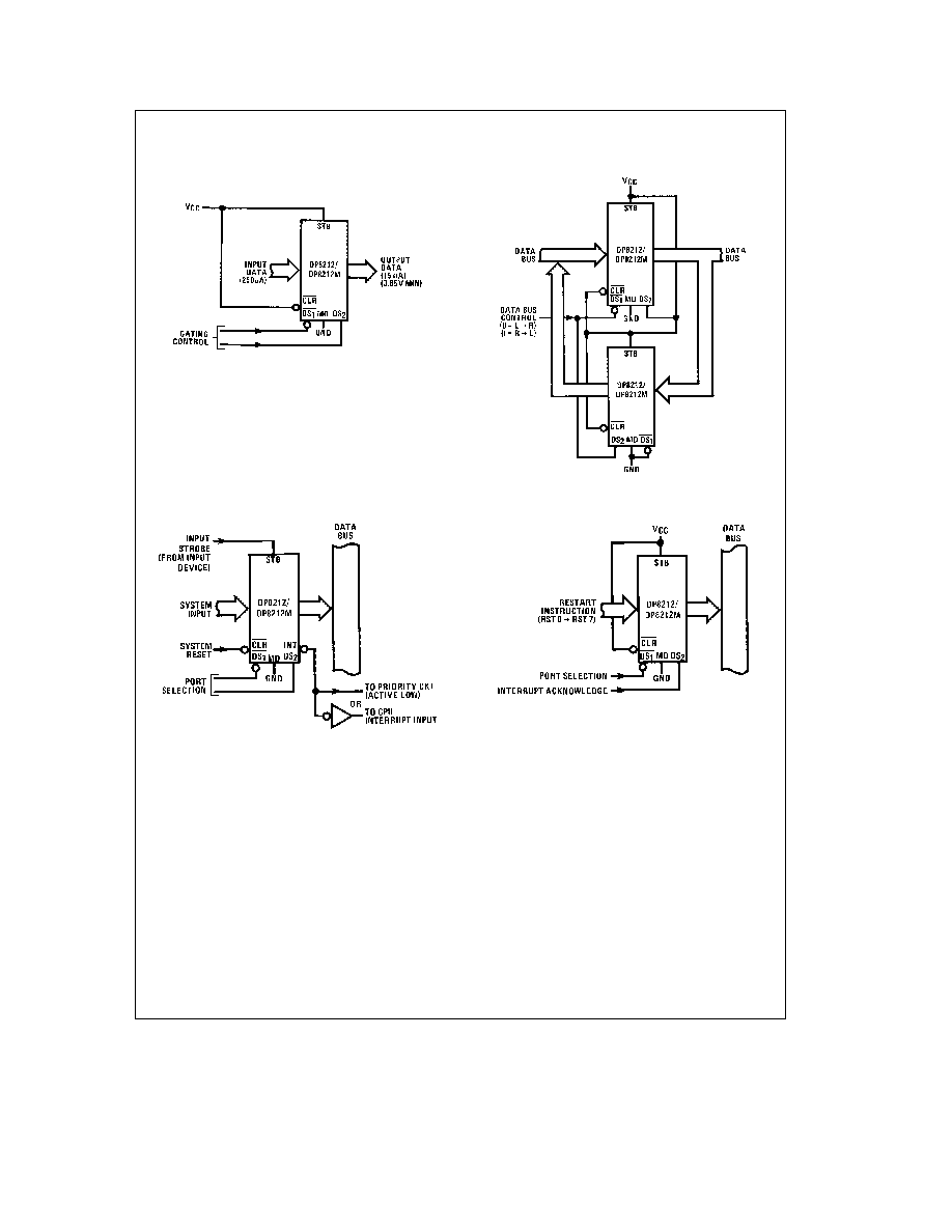
Applications in Microcomputer Systems
Gated Buffer
(TRI-STATE)
TL F 6824 � 7
TL F 6824 � 8
Interrupting Input Port
TL F 6824 � 9
Interrupt Instruction Port
TL F 6824 � 10
7
Applications in Microcomputer Systems
(Continued)
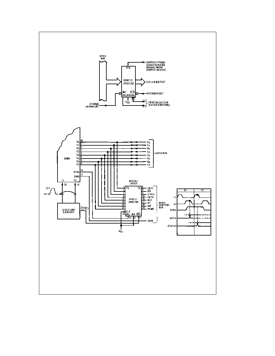
Output Port (with Hand-Shanking)
TL F 6824 � 11
INS8080A Status Latch
TL F 6824 � 12
8
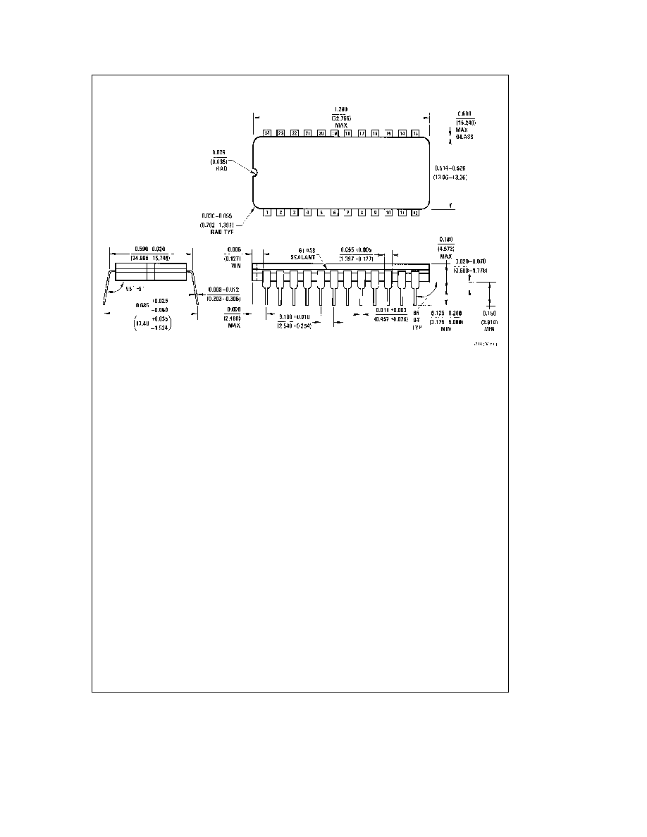
Physical Dimensions
inches (millimeters)
Ceramic Dual-In-Line Package (J)
Order Number DP8212J or DP8212MJ
NS Package Number J24A
9
DP8212DP8212M
8-Bit
InputOutput
Port
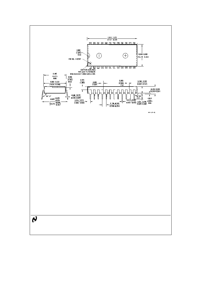
Physical Dimensions
inches (millimeters) (Continued)
Molded Dual-In-Line Package (N)
Order Number DP8212N
NS Package Number N24A
LIFE SUPPORT POLICY
NATIONAL'S PRODUCTS ARE NOT AUTHORIZED FOR USE AS CRITICAL COMPONENTS IN LIFE SUPPORT
DEVICES OR SYSTEMS WITHOUT THE EXPRESS WRITTEN APPROVAL OF THE PRESIDENT OF NATIONAL
SEMICONDUCTOR CORPORATION As used herein
1 Life support devices or systems are devices or
2 A critical component is any component of a life
systems which (a) are intended for surgical implant
support device or system whose failure to perform can
into the body or (b) support or sustain life and whose
be reasonably expected to cause the failure of the life
failure to perform when properly used in accordance
support device or system or to affect its safety or
with instructions for use provided in the labeling can
effectiveness
be reasonably expected to result in a significant injury
to the user
National Semiconductor
National Semiconductor
National Semiconductor
National Semiconductor
Corporation
Europe
Hong Kong Ltd
Japan Ltd
1111 West Bardin Road
Fax (a49) 0-180-530 85 86
13th Floor Straight Block
Tel 81-043-299-2309
Arlington TX 76017
Email cnjwge tevm2 nsc com
Ocean Centre 5 Canton Rd
Fax 81-043-299-2408
Tel 1(800) 272-9959
Deutsch Tel (a49) 0-180-530 85 85
Tsimshatsui Kowloon
Fax 1(800) 737-7018
English
Tel (a49) 0-180-532 78 32
Hong Kong
Fran ais Tel (a49) 0-180-532 93 58
Tel (852) 2737-1600
Italiano
Tel (a49) 0-180-534 16 80
Fax (852) 2736-9960
National does not assume any responsibility for use of any circuitry described no circuit patent licenses are implied and National reserves the right at any time without notice to change said circuitry and specifications